BGA2816,115 NXP Semiconductors, BGA2816,115 Datasheet
BGA2816,115
Specifications of BGA2816,115


Related parts for BGA2816,115


BGA2816,115 Summary of contents
Page 1
BGA2816 MMIC wideband amplifier Rev. 2 — 29 October 2010 1. Product profile 1.1 General description Silicon Monolithic Microwave Integrated Circuit (MMIC) wideband amplifier with internal matching circuit in a 6-pin SOT363 plastic SMD package. 1.2 Features and benefits Input ...
Page 2
... NXP Semiconductors 3. Ordering information Table 2. Type number BGA2816 4. Marking Table 3. Type number BGA2816 5. Limiting values Table 4. In accordance with the Absolute Maximum Rating System (IEC 60134). Symbol tot T stg drive 6. Thermal characteristics Table 5. Symbol R th(j-sp) 7. Characteristics Table 6. Characteristics Ω 3 Symbol Parameter ...
Page 3
... NXP Semiconductors Table 6. Characteristics …continued Ω 3 Symbol Parameter G power gain p RL input return loss in RL output return loss out ISL isolation NF noise figure −3 dB bandwidth B −3dB K Rollett stability factor P saturated output power L(sat) P output power gain compression f = 250 MHz L(1dB) IP3 ...
Page 4
... NXP Semiconductors 8. Application information Figure 1 internally matched to 50 Ω and therefore does not need any external matching. The value of the input and output DC blocking capacitors C2 and C3 should not be more than 100 pF for applications above 100 MHz. However, when the device is operated below 100 MHz, the capacitor value should be increased ...
Page 5
... NXP Semiconductors 8.2 Graphs ( 250 MHz ( 950 MHz ( 2150 MHz Fig 4. BGA2816 Product data sheet 135° +0.5 +0.2 0 0.2 0.5 180° −0.2 −0.5 −135° ° 21 amb CC CC Input reflection coefficient (S ); typical values 11 All information provided in this document is subject to legal disclaimers. ...
Page 6
... NXP Semiconductors ( 250 MHz ( 950 MHz ( 2150 MHz Fig 5. BGA2816 Product data sheet 135° +0.5 +0.2 0 0.2 0.5 180° −0.2 −0.5 −135° ° 21 amb CC CC Output reflection coefficient (S 22 All information provided in this document is subject to legal disclaimers. ...
Page 7
... NXP Semiconductors − −39 dBm Ω. P drive ° amb = −40 ° amb = 25 ° amb = 85 ° amb = −40 ° amb Fig 6. Rollett stability factor as function of frequency; typical values BGA2816 Product data sheet 001aam275 (1) (3) (4) (2) ( (GHz) = 18. ...
Page 8
... NXP Semiconductors 0 RL out (dB) −10 −20 − −39 dBm Ω. P drive ° amb = −40 ° amb = 25 ° amb = 85 ° amb = −40 ° amb Fig 8. Output return loss as function of frequency; typical values BGA2816 Product data sheet 001aam277 ...
Page 9
... NXP Semiconductors 0 ISL (dB) −20 −40 −60 − −40 dBm Ω. P drive ° amb = −40 ° amb = 25 ° amb = 85 ° amb = −40 ° amb Fig 10. Isolation as function of frequency; typical values 8.3 Tables Table 7. Typical values. Symbol I CC Table 8 ...
Page 10
... NXP Semiconductors Table 9. Typical values. Symbol Parameter P i(1dB) Table 10. Typical values. Symbol P L(1dB) BGA2816 Product data sheet Input power gain compression over temperature and supply voltages input power gain compression Output power gain compression over temperature and supply voltages Parameter output power gain compression All information provided in this document is subject to legal disclaimers. Rev. 2 — ...
Page 11
... NXP Semiconductors Table 11. Typical values. Symbol P L(sat) Table 12. Typical values. Symbol ΔIM2 BGA2816 Product data sheet Saturated output power over temperature and supply voltages Parameter saturated output power Second-order intermodulation distance over temperature and supply voltages Parameter second-order intermodulation distance All information provided in this document is subject to legal disclaimers. ...
Page 12
... NXP Semiconductors Table 13. Typical values. Symbol IP3 O Table 14. Typical values. Symbol B −3dB BGA2816 Product data sheet Output third-order intercept point over temperature and supply voltages Parameter output third-order intercept point −3 dB bandwidth over temperature and supply voltages Parameter Conditions −3 dB bandwidth ...
Page 13
... NXP Semiconductors 9. Test information 30 mm True size = 30 mm × 30 mm. Fig 12. PCB layout and demo board with components Table 15. Component C1 IC1 BGA2816 Product data sheet 30 mm List of components used for the typical application Description multilayer ceramic chip capacitor multilayer ceramic chip capacitor BGA2816 MMIC All information provided in this document is subject to legal disclaimers ...
Page 14
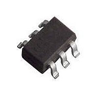
... NXP Semiconductors 10. Package outline Plastic surface-mounted package; 6 leads y 6 pin 1 index DIMENSIONS (mm are the original dimensions UNIT max 1.1 0.30 0.25 mm 0.1 0.8 0.20 0.10 OUTLINE VERSION IEC SOT363 Fig 13. Package outline SOT363 BGA2816 Product data sheet scale 2.2 1.35 2.2 1 ...
Page 15
... NXP Semiconductors 11. Abbreviations Table 16. Acronym DC IF LNA LNB PCB RF SMD 12. Revision history Table 17. Revision history Document ID Release date BGA2816 v.2 20101029 • Modifications Table 4 on page BGA2816 v.1 20100830 BGA2816 Product data sheet Abbreviations Description Direct Current Intermediate Frequency Low-Noise Amplifier ...
Page 16
... In no event shall NXP Semiconductors be liable for any indirect, incidental, punitive, special or consequential damages (including - without limitation - lost profits, lost savings, business interruption, costs related to the removal or ...
Page 17
... Product data sheet NXP Semiconductors’ specifications such use shall be solely at customer’s own risk, and (c) customer fully indemnifies NXP Semiconductors for any liability, damages or failed product claims resulting from customer design and use of the product for automotive applications beyond NXP Semiconductors’ ...
Page 18
... NXP Semiconductors 15. Contents 1 Product profile . . . . . . . . . . . . . . . . . . . . . . . . . . 1 1.1 General description . . . . . . . . . . . . . . . . . . . . . 1 1.2 Features and benefits . . . . . . . . . . . . . . . . . . . . 1 1.3 Applications . . . . . . . . . . . . . . . . . . . . . . . . . . . 1 2 Pinning information . . . . . . . . . . . . . . . . . . . . . . 1 3 Ordering information . . . . . . . . . . . . . . . . . . . . . 2 4 Marking . . . . . . . . . . . . . . . . . . . . . . . . . . . . . . . . 2 5 Limiting values Thermal characteristics . . . . . . . . . . . . . . . . . . 2 7 Characteristics . . . . . . . . . . . . . . . . . . . . . . . . . . 2 8 Application information 8.1 Application examples . . . . . . . . . . . . . . . . . . . . 4 8.2 Graphs . . . . . . . . . . . . . . . . . . . . . . . . . . . . . . . 5 8.3 Tables . . . . . . . . . . . . . . . . . . . . . . . . . . . . . . . . 9 9 Test information . . . . . . . . . . . . . . . . . . . . . . . . 13 10 Package outline ...