ATAKSTK511-3 Atmel, ATAKSTK511-3 Datasheet - Page 26
ATAKSTK511-3
Manufacturer Part Number
ATAKSTK511-3
Description
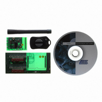
KIT RF MODULE 315MHZ FOR STK500
Manufacturer
Atmel
Series
SmartRF®r
Type
Transmitter, Receiver, ASK, FSKr
Specifications of ATAKSTK511-3
Frequency
433MHz
Wireless Frequency
315 MHz
For Use With/related Products
ATSTK500
Lead Free Status / RoHS Status
Contains lead / RoHS non-compliant
Other names
Q2262874


5.1.4
STK511 User Guide
Circuit Description
Multi-function Ports: The ATtiny13 has excellent I/O capabilities, despite its 8-pin packaging, due to
multiple functionality of each I/O pin (excluding V
ming, external (pin-change) interrupts, analog signal input, external clock input, and many other features
are possible.
Low-current Sleep Mode: Three levels of sleep are possible with the ATtiny13, each offering a different
combination of in-sleep/wake-up capabilities and current-saving options. One configuration, as demon-
strated in the accompanying demo software, permits the ATtiny13 to draw less than 1 µA of current while
asleep.
Internal RC Oscillator: The ATtiny13 contains a fuse-selectable, calibrated internal RC oscillator, which
provides a 4.8 MHz or 9.6 MHz clock. No external components are required. The accuracy of the oscilla-
tor is ±10% of the nominal frequency. Atmel Application Note AVR053 outlines a method to re-calibrate
the oscillator to an accuracy approaching ±1%.
External Clock Input: In addition to an internal RC oscillator clock source, the ATtiny13 can accept an
external clock signal. The T575x transmitter ICs can provide this buffered clock if a 0- resistor is
installed at the R1 location on the transmitter application board. The frequency of this T575x-supplied
clock is f
Button-inputs S1 and S2: Two button inputs allow the user to control the function of the transmitter.
These button inputs are connected between ports PB1/PB2 of the ATtiny13 and the +3 V supply. Ini-
tially, these ports are set as input, a hi-Z tristate condition. The voltage level on these ports is held low by
the two 220k resistors, R7 and R8, to ground. This is necessary because the voltage at the T575x
PA_ENABLE port must be < 0.25 V to remain low, or else RF energy could be inadvertently radiated.
Resistors R2 and R6 limit the current into these two ports. When a button is pushed, the +3 V supply
(through the R6/R7 or R2/R8 voltage divider) is presented to the corresponding port (PB1 or PB2,
respectively). This change in level on the port pin is sensed by the microcontroller and a pin-change
interrupt is generated. Firmware then directs the microcontroller to the appropriate Interrupt Service
Routine vector.
Indicator LEDs: Activity on switches S1 and S2, as well as the port states of PB1 and PB2 (such as
transmitter activation, or ASK/FSK modulation), is indicated on these LEDs. R4 and R9 are source-cur-
rent-limiting resistors.
A/D Converter: The ATtiny13 has a built-in 10-bit A/D converter. The STK511 transmitter demonstrates
the capability of this ADC with a CdS cell incorporated as a light-intensity sensor. This cell has a dark
resistance of ~200 k and an illuminated resistance < 100 . In the circuit, resistor R3 sets the bias from
port PB4 (when set to output high) on the CdS cell. R3 is also a part of a voltage divider with R5 that
determines the input voltage range to the ADC port (PB3). In addition, the parallel resistance of R5 and
the CdS cell is calculated to provide a range of ~0 V up to 1.1 V to the ADC input (1.1 V is the internal
voltage reference value for the ADC).
Antenna: The STK511 transmitter incorporates a PC-board-trace loop antenna. The antenna is driven
by the single-ended output of the T575x through port ANT1. Bias voltage for the T575x’s power amplifier
is fed to ANT1 through a printed-trace inductor of 50 mH-100 mH, L2. At the output of the T575x, C2,
C10, and L2 form a matching network, which can be set-up as a C, L, LC, or
are additional matching capacitors, which compensate for the inductance of the loop. The optimum load
(ie, antenna) impedance for the T5750/3/4 can be found in the respective IC’s documentation.
XTAL
/4.
CC
and GND). Because of this flexibility, ISP program-
STK511 Transmitter Board
configuration. C4 and C5
4842B–AVR–10/09
5-3
Related parts for ATAKSTK511-3
Image
Part Number
Description
Manufacturer
Datasheet
Request
R

Part Number:
Description:
DEV KIT FOR AVR/AVR32
Manufacturer:
Atmel
Datasheet:

Part Number:
Description:
INTERVAL AND WIPE/WASH WIPER CONTROL IC WITH DELAY
Manufacturer:
ATMEL Corporation
Datasheet:
Part Number:
Description:
Low-Voltage Voice-Switched IC for Hands-Free Operation
Manufacturer:
ATMEL Corporation
Datasheet:
Part Number:
Description:
MONOLITHIC INTEGRATED FEATUREPHONE CIRCUIT
Manufacturer:
ATMEL Corporation
Datasheet:
Part Number:
Description:
AM-FM Receiver IC U4255BM-M
Manufacturer:
ATMEL Corporation
Datasheet:
Part Number:
Description:
Monolithic Integrated Feature Phone Circuit
Manufacturer:
ATMEL Corporation
Datasheet:
Part Number:
Description:
Multistandard Video-IF and Quasi Parallel Sound Processing
Manufacturer:
ATMEL Corporation
Datasheet:
Part Number:
Description:
High-performance EE PLD
Manufacturer:
ATMEL Corporation
Datasheet:
Part Number:
Description:
8-bit Flash Microcontroller
Manufacturer:
ATMEL Corporation
Datasheet:
Part Number:
Description:
2-Wire Serial EEPROM
Manufacturer:
ATMEL Corporation
Datasheet: