MLX71121KLQ Melexis Inc, MLX71121KLQ Datasheet - Page 11
MLX71121KLQ
Manufacturer Part Number
MLX71121KLQ
Description
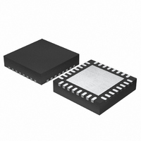
RCVR FSK/FM/ASK 32-QFN
Manufacturer
Melexis Inc
Specifications of MLX71121KLQ
Frequency
300MHz ~ 930MHz
Sensitivity
-108dBm
Data Rate - Maximum
100 kbps
Modulation Or Protocol
ASK, FM, FSK
Applications
General Remote Control, Garage Opener, RKE
Current - Receiving
8.1mA
Data Interface
PCB, Surface Mount
Antenna Connector
PCB, Surface Mount
Features
RSSI Equipped
Voltage - Supply
2.1 V ~ 5.5 V
Operating Temperature
-40°C ~ 125°C
Package / Case
32-QFN
Data Rate
100Kbps
Frequency Range
300MHz To 930MHz
Modulation Type
AM, FM, FSK
Rf Ic Case Style
QFN
No. Of Pins
32
Supply Voltage Range
2.1V To 5.5V
Operating Temperature Range
-40°C To
Sensitivity Dbm
-112dBm
Rohs Compliant
Yes
Lead Free Status / RoHS Status
Lead free / RoHS Compliant
Memory Size
-
Lead Free Status / RoHS Status
Lead free / RoHS Compliant, Lead free / RoHS Compliant
Other names
MLX71121A
Available stocks
Company
Part Number
Manufacturer
Quantity
Price
Company:

Part Number:
MLX71121KLQ
Manufacturer:
TOSHIBA
Quantity:
3 000


1.14.1
The simplest configuration is the averaging or RC inte-
gration method. Here an on-chip 100kΩ resistor to-
gether with an external slicer capacitor (CSL) are form-
ing an RC low-pass filter. This way the threshold voltage
automatically adjusts to the mean or average value of
the analog input voltage.
To create a stable threshold voltage, the cut-off fre-
quency of the low pass has to be lower than the lowest
signal frequency.
A long string of zeros or ones, like in NRZ codes, can
cause a drift of the threshold. That’s why a Manchester
or other DC-free coding scheme works best.
The peak detectors are disabled during averaging de-
tection mode, and the output pins PDP and PDN are
pulled to ground (S4, S6 are closed).
1.14.2
Peak detection mode has a general advantage over
averaging detection mode because of the part attack
and slow release times. Peak detection should be used
for all non DC-free codes like NRZ. In this configuration
the threshold is generated by using the positive and
negative peak detectors. The slicer comparator thresh-
old is set to the midpoint between the high output and
the low output of the data filter by an on-chip resistance
divider. Two external capacitors (CP1, CP2) determine
the release times for the positive and negative enve-
lope. The two on-chip resistors provide a path for the
capacitors to discharge. This allows the peak detectors
to dynamically follow peak changes of the data filter
output voltage. The attack times are very short due to
the high peak detector load currents of about 500uA.
The decay time constant mainly depends on the longest
time period without bit polarity change. This corre-
sponds to the maximum number of consecutive bits with
the same polarity (N
If the receiver is in shutdown mode and peak detection mode is selected then the peak detectors are dis-
abled and the output of the positive peak detector (PDP) is connected to VEE (S4 is closed) and the output
of the negative peak detector (PDN) is connected to VCC (S5 is closed). This guarantees the correct biasing
of CP1 and CP2 during start-up.
39010 71121
Rev. 009
CSL
CP1/2
≥
≥
100k
τ
Averaging Detection Mode
Peak Detection Mode
AVG
τ
100k
DECAY
MAX
).
τ
τ
AVG
DECAY
=
=
R
1.5
RZ
N
R
MAX
NRZ
Page 11 of 28
Fig. 7:
Fig. 8:
SLCSEL
SLCSEL
filter
data
filter
data
Data path in averaging detection mode
Data path in peak detection mode
FSK/FM/ASK Receiver
100k
PKDET _
OA2
100k
PKDET _
OA2
PKDET+
PKDET+
MLX71121
switches
switches
S2
S2
300 to 930MHz
Control
Control
logic
logic
data slicer
data slicer
S1
S3
S1
S3
VCC
VCC
S4
S5
S6
S4
S5
S6
Data Sheet
SLC
PDN
DTAO
CINT
PDP
SLC
PDN
PDP
DTAO
CINT
Oct/10
CP1
CP2
CSL
Related parts for MLX71121KLQ
Image
Part Number
Description
Manufacturer
Datasheet
Request
R

Part Number:
Description:
IC LATCH CMOS MP TSOT23-3
Manufacturer:
Melexis Inc
Datasheet:

Part Number:
Description:
IC LATCH CMOS MP TSOT23-3
Manufacturer:
Melexis Inc
Datasheet:

Part Number:
Description:
IC HALL EFFECT SW TSOT-23
Manufacturer:
Melexis Inc
Datasheet:

Part Number:
Description:
IC HALL EFFECT SWITCH TSOT-23
Manufacturer:
Melexis Inc
Datasheet:

Part Number:
Description:
IC HALL EFFECT SW
Manufacturer:
Melexis Inc
Datasheet:

Part Number:
Description:
IC HALL EFFECT SWITCH TSOT-23
Manufacturer:
Melexis Inc
Datasheet:

Part Number:
Description:
IC HALL EFFECT SWITCH TSOT-23
Manufacturer:
Melexis Inc
Datasheet:

Part Number:
Description:
IC LATCH CMOS MP TO-92UA
Manufacturer:
Melexis Inc
Datasheet: