MLX71121KLQ Melexis Inc, MLX71121KLQ Datasheet - Page 12
MLX71121KLQ
Manufacturer Part Number
MLX71121KLQ
Description
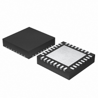
RCVR FSK/FM/ASK 32-QFN
Manufacturer
Melexis Inc
Specifications of MLX71121KLQ
Frequency
300MHz ~ 930MHz
Sensitivity
-108dBm
Data Rate - Maximum
100 kbps
Modulation Or Protocol
ASK, FM, FSK
Applications
General Remote Control, Garage Opener, RKE
Current - Receiving
8.1mA
Data Interface
PCB, Surface Mount
Antenna Connector
PCB, Surface Mount
Features
RSSI Equipped
Voltage - Supply
2.1 V ~ 5.5 V
Operating Temperature
-40°C ~ 125°C
Package / Case
32-QFN
Data Rate
100Kbps
Frequency Range
300MHz To 930MHz
Modulation Type
AM, FM, FSK
Rf Ic Case Style
QFN
No. Of Pins
32
Supply Voltage Range
2.1V To 5.5V
Operating Temperature Range
-40°C To
Sensitivity Dbm
-112dBm
Rohs Compliant
Yes
Lead Free Status / RoHS Status
Lead free / RoHS Compliant
Memory Size
-
Lead Free Status / RoHS Status
Lead free / RoHS Compliant, Lead free / RoHS Compliant
Other names
MLX71121A
Available stocks
Company
Part Number
Manufacturer
Quantity
Price
Company:

Part Number:
MLX71121KLQ
Manufacturer:
TOSHIBA
Quantity:
3 000


1.15 Noise Cancellation Filter and Data Output
The data output pin DTAO delivers the demodulated data signal which can be further processed by a noise
cancellation filter (NCF). The NCF can be disabled if pin CINT is connected to ground. In this case the
multiplexer (MUX) connects the receiver output DTAO directly to the data slicer output.
Fig. 9:
The noise cancellation filter can suppress random pulses in the data output which are shorter than t
The NCF can also operate as a muting circuit. So if the RF input signal is below sensitivity level (or if no
RF signal is applied) then the data output will go to a constant DC level (either HIGH or LOW). This can be
achieved by setting the bandwidth of the preceding data filter (sec 1.13) about 10 times higher than the
bandwidth of the NCF.
Having the NCF activated is a good means for reducing the computing power of the microcontroller that fol-
lows the receiver IC for further data processing.
In contrast to a conventional muting (or squelch) circuit, this topology does not need the RSSI signal for level
indication. The filtering process is done by means of an analogue integrator. The cut-off frequency of the
NCF is set by the external capacitor connected to pin CINT. This capacitor C
the maximum data rate. Below table provides some recommendations..
During receiver start-up a sequencer checks if pin CINT is connected to a capacitor or to ground. The maxi-
mum value of C
noise cancellation filter is activated.
In shutdown mode pin DTAO is set to Hi-Z state.
39010 71121
Rev. 009
CF3
=
15
Data output and noise filter
⋅
10
R
6 -
RZ
data slicer
⋅
F3
output
[kbit/s]
0.6
1.2
1.6
2.4
3.3
4.8
6.0
t
min
should not exceed 12nF. This defines the lowest data rate that can be processed if the
=
15
noise cancellation filter
R
⋅
NRZ
10
NCF
−
6
=
MUX
7
5 .
R
⋅
RZ
10
−
6
DTAO
CINT
Page 12 of 28
R
CF3
NRZ
1.2
2.4
3.2
4.8
6.6
9.6
12
[kbit/s]
FSK/FM/ASK Receiver
F3
should be set according to
MLX71121
C
300 to 930MHz
F3
6.8
4.7
3.3
2.2
1.5
1.2
12
[nF]
Data Sheet
min
.
Oct/10
Related parts for MLX71121KLQ
Image
Part Number
Description
Manufacturer
Datasheet
Request
R

Part Number:
Description:
IC LATCH CMOS MP TSOT23-3
Manufacturer:
Melexis Inc
Datasheet:

Part Number:
Description:
IC LATCH CMOS MP TSOT23-3
Manufacturer:
Melexis Inc
Datasheet:

Part Number:
Description:
IC HALL EFFECT SW TSOT-23
Manufacturer:
Melexis Inc
Datasheet:

Part Number:
Description:
IC HALL EFFECT SWITCH TSOT-23
Manufacturer:
Melexis Inc
Datasheet:

Part Number:
Description:
IC HALL EFFECT SW
Manufacturer:
Melexis Inc
Datasheet:

Part Number:
Description:
IC HALL EFFECT SWITCH TSOT-23
Manufacturer:
Melexis Inc
Datasheet:

Part Number:
Description:
IC HALL EFFECT SWITCH TSOT-23
Manufacturer:
Melexis Inc
Datasheet:

Part Number:
Description:
IC LATCH CMOS MP TO-92UA
Manufacturer:
Melexis Inc
Datasheet: