MLX71121KLQ Melexis Inc, MLX71121KLQ Datasheet - Page 6
MLX71121KLQ
Manufacturer Part Number
MLX71121KLQ
Description
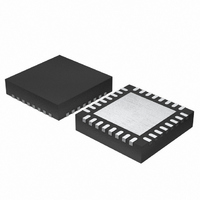
RCVR FSK/FM/ASK 32-QFN
Manufacturer
Melexis Inc
Specifications of MLX71121KLQ
Frequency
300MHz ~ 930MHz
Sensitivity
-108dBm
Data Rate - Maximum
100 kbps
Modulation Or Protocol
ASK, FM, FSK
Applications
General Remote Control, Garage Opener, RKE
Current - Receiving
8.1mA
Data Interface
PCB, Surface Mount
Antenna Connector
PCB, Surface Mount
Features
RSSI Equipped
Voltage - Supply
2.1 V ~ 5.5 V
Operating Temperature
-40°C ~ 125°C
Package / Case
32-QFN
Data Rate
100Kbps
Frequency Range
300MHz To 930MHz
Modulation Type
AM, FM, FSK
Rf Ic Case Style
QFN
No. Of Pins
32
Supply Voltage Range
2.1V To 5.5V
Operating Temperature Range
-40°C To
Sensitivity Dbm
-112dBm
Rohs Compliant
Yes
Lead Free Status / RoHS Status
Lead free / RoHS Compliant
Memory Size
-
Lead Free Status / RoHS Status
Lead free / RoHS Compliant, Lead free / RoHS Compliant
Other names
MLX71121A
Available stocks
Company
Part Number
Manufacturer
Quantity
Price
Company:

Part Number:
MLX71121KLQ
Manufacturer:
TOSHIBA
Quantity:
3 000


1.4
The receiver offers two operating modes selectable by setting the corresponding logic level at pin ENRX.
Note: ENRX is pulled down internally.
The receiver’s start-up procedure is controlled by a sequencer circuit. It performs the sequential activation of
the different building blocks. It also initiates the pre-charging of the data filter and data slicer capacitors in
order to reduce the overall start-up time and current consumption during the start-up phase.
At ENRX = 0, the receiver is in shutdown mode and draws only a few nA. The bias system and the reference
oscillator are activated after enabling the receiver by a positive edge at pin ENRX. The crystal oscillator (RO)
is turned on first. Then the crystal oscillation amplitude builds up from noise. After reaching a certain ampli-
tude level at pin ROI, the whole IC is activated and draws the full receive mode current consumption I
This event is used to start the pre-charging of the external data path capacitors. Pre-charging is finished
after 5504 clock cycles. After that time the data output pin DTAO output is activated.
1.5
The receiver features two identical LNAs. Each LNA is a cascode amplifier with a voltage gain of approxi-
mately 18dB. The actual gain depends on the antenna matching network at the inputs and the LC tank net-
work between the LNA outputs and mixer input. LNA operation can be controlled by the LNASEL pin.
Pin LNASEL is internally pulled to VCC/2 during receive mode. Therefore both LNAs are active if LNASEL is
left floating (Hi-Z state).
39010 71121
Rev. 009
ENRX
DTAO
I
I
I
Operating Modes
LNA Selection
SDN
CC
RO
LNASEL
ENRX
Hi-Z
0
1
0
1
t
Hi-Z
on RO
Fig. 2:
t
on RX
t
SEQ
Timing diagram of start-up and shutdown behavior
Page 6 of 28
LNA1 active, LNA2 shutdown
LNA1 shutdown, LNA2 active
LNA1 and LNA2 active
Shutdown mode
Receive mode
valid data
Description
Description
FSK/FM/ASK Receiver
MLX71121
300 to 930MHz
Hi-Z
Data Sheet
Oct/10
CC
.
Related parts for MLX71121KLQ
Image
Part Number
Description
Manufacturer
Datasheet
Request
R

Part Number:
Description:
IC LATCH CMOS MP TSOT23-3
Manufacturer:
Melexis Inc
Datasheet:

Part Number:
Description:
IC LATCH CMOS MP TSOT23-3
Manufacturer:
Melexis Inc
Datasheet:

Part Number:
Description:
IC HALL EFFECT SW TSOT-23
Manufacturer:
Melexis Inc
Datasheet:

Part Number:
Description:
IC HALL EFFECT SWITCH TSOT-23
Manufacturer:
Melexis Inc
Datasheet:

Part Number:
Description:
IC HALL EFFECT SW
Manufacturer:
Melexis Inc
Datasheet:

Part Number:
Description:
IC HALL EFFECT SWITCH TSOT-23
Manufacturer:
Melexis Inc
Datasheet:

Part Number:
Description:
IC HALL EFFECT SWITCH TSOT-23
Manufacturer:
Melexis Inc
Datasheet:

Part Number:
Description:
IC LATCH CMOS MP TO-92UA
Manufacturer:
Melexis Inc
Datasheet: