ATMEGA64RZAV-10PU Atmel, ATMEGA64RZAV-10PU Datasheet - Page 93
ATMEGA64RZAV-10PU
Manufacturer Part Number
ATMEGA64RZAV-10PU
Description
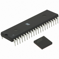
MCU ATMEGA644/AT86RF230 40-DIP
Manufacturer
Atmel
Series
ATMEGAr
Datasheets
1.ATMEGA644-20MU.pdf
(23 pages)
2.ATMEGA644-20MU.pdf
(376 pages)
3.AT86RF230-ZU.pdf
(98 pages)
Specifications of ATMEGA64RZAV-10PU
Frequency
2.4GHz
Modulation Or Protocol
802.15.4 Zigbee
Power - Output
3dBm
Sensitivity
-101dBm
Voltage - Supply
1.8 V ~ 3.6 V
Data Interface
PCB, Surface Mount
Memory Size
64kB Flash, 2kB EEPROM, 4kB RAM
Antenna Connector
PCB, Surface Mount
Package / Case
40-DIP (0.600", 15.24mm)
Wireless Frequency
2.4 GHz
Interface Type
JTAG, SPI
Output Power
3 dBm
For Use With
ATSTK600-TQFP32 - STK600 SOCKET/ADAPTER 32-TQFPATAVRISP2 - PROGRAMMER AVR IN SYSTEMATSTK500 - PROGRAMMER AVR STARTER KIT
Lead Free Status / RoHS Status
Lead free / RoHS Compliant
Operating Temperature
-
Applications
-
Data Rate - Maximum
-
Current - Transmitting
-
Current - Receiving
-
Lead Free Status / Rohs Status
Lead free / RoHS Compliant
For Use With/related Products
ATmega64


Table of Contents
5131E-MCU Wireless-02/09
1 Pin-out Diagram ..................................................................................2
Disclaimer...............................................................................................2
2 Overview ..............................................................................................2
3 General Circuit Description................................................................3
4 Pin Description....................................................................................4
5 Application Circuit ..............................................................................8
6 Microcontroller Interface ..................................................................10
7 Operating Modes...............................................................................21
8 Functional Description .....................................................................45
4.1 Supply and Ground Pins ........................................................................................ 4
4.2 Analog and RF Pins ............................................................................................... 5
4.3 Digital Pins.............................................................................................................. 6
6.1 SPI Timing Description......................................................................................... 11
6.2 SPI Protocol.......................................................................................................... 12
6.3 Radio Transceiver Identification ........................................................................... 16
6.4 Sleep/Wake-up and Transmit Signal (SLP_TR)................................................... 17
6.5 Interrupt Logic....................................................................................................... 19
7.1 Basic Operating Mode.......................................................................................... 21
7.2 Extended Operating Mode ................................................................................... 29
8.1 Introduction - Frame Format................................................................................. 45
4.3.1 Driver Strength Settings of Digital Output Pins.............................................................. 6
4.3.2 Pull-up and Pull-down Configuration of Digital Input Pins.............................................. 7
4.3.3 Register Description ...................................................................................................... 7
6.2.1 Register Access Mode................................................................................................. 12
6.2.2 Frame Buffer Access Modes ....................................................................................... 13
6.2.3 SRAM Access Mode.................................................................................................... 14
6.3.1 Register Description .................................................................................................... 16
6.5.1 Overview ..................................................................................................................... 19
6.5.2 Register Description .................................................................................................... 20
7.1.1 State Control ............................................................................................................... 21
7.1.2 Basic Operating Mode Description .............................................................................. 22
7.1.3 Interrupt Handling in Basic Operating Mode................................................................ 24
7.1.4 Basic Mode Timing ...................................................................................................... 25
7.1.5 Register Description .................................................................................................... 27
7.2.1 State Control ............................................................................................................... 31
7.2.2 Configuration ............................................................................................................... 32
7.2.3 Extended Operating Mode Description........................................................................ 33
7.2.4 Interrupt Handling in Extended Operating Mode ......................................................... 37
7.2.5 Register Summary....................................................................................................... 38
7.2.6 Register Description – Control Registers..................................................................... 38
7.2.7 Register Description – Address Registers ................................................................... 42
8.1.1 PHY Protocol Layer Data Unit (PPDU)........................................................................ 45
AT86RF230
93
Related parts for ATMEGA64RZAV-10PU
Image
Part Number
Description
Manufacturer
Datasheet
Request
R

Part Number:
Description:
DEV KIT FOR AVR/AVR32
Manufacturer:
Atmel
Datasheet:

Part Number:
Description:
INTERVAL AND WIPE/WASH WIPER CONTROL IC WITH DELAY
Manufacturer:
ATMEL Corporation
Datasheet:
Part Number:
Description:
Low-Voltage Voice-Switched IC for Hands-Free Operation
Manufacturer:
ATMEL Corporation
Datasheet:
Part Number:
Description:
MONOLITHIC INTEGRATED FEATUREPHONE CIRCUIT
Manufacturer:
ATMEL Corporation
Datasheet:
Part Number:
Description:
AM-FM Receiver IC U4255BM-M
Manufacturer:
ATMEL Corporation
Datasheet:
Part Number:
Description:
Monolithic Integrated Feature Phone Circuit
Manufacturer:
ATMEL Corporation
Datasheet:
Part Number:
Description:
Multistandard Video-IF and Quasi Parallel Sound Processing
Manufacturer:
ATMEL Corporation
Datasheet:
Part Number:
Description:
High-performance EE PLD
Manufacturer:
ATMEL Corporation
Datasheet:
Part Number:
Description:
8-bit Flash Microcontroller
Manufacturer:
ATMEL Corporation
Datasheet:
Part Number:
Description:
2-Wire Serial EEPROM
Manufacturer:
ATMEL Corporation
Datasheet: