SPBT2532C2.AT STMicroelectronics, SPBT2532C2.AT Datasheet - Page 13
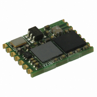
SPBT2532C2.AT
Manufacturer Part Number
SPBT2532C2.AT
Description
IC BLUETOOTH VER 2.1 CLASS 2
Manufacturer
STMicroelectronics
Datasheets
1.STEVAL-SPBT2ATV1.pdf
(50 pages)
2.SPBT2532C2.AT.pdf
(2 pages)
3.SPBT2532C2.AT.pdf
(55 pages)
Specifications of SPBT2532C2.AT
Frequency
2.4GHz
Data Rate - Maximum
2Mbps
Modulation Or Protocol
Bluetooth v2.1+EDR, Class 2 & 3
Applications
General Purpose
Power - Output
2dBm
Sensitivity
-85dBm
Voltage - Supply
2.8 V ~ 3.6 V
Data Interface
PCB, Surface Mount
Memory Size
256kB Flash, 48kB RAM
Antenna Connector
PCB, Surface Mount
Operating Temperature
-40°C ~ 85°C
Package / Case
Module
Wireless Frequency
2400 MHz to 2483.5 MHz
Interface Type
I2C, I2S, SPI, UART
Data Rate
2 Mbps
Modulation
AFH
Operating Voltage
2.8 V to 3.6 V
Antenna
Without Antenna
Board Size
10 mm x 13 mm
Operating Temperature Range
- 40 C to + 85 C
Output Power
4 mA
Security
128 bit Encryption
Technology/ Type
Class 2 Bluetooth Module
Processor Series
STLC2500
For Use With
497-10656 - BOARD DEMO BLUETOOTH SPBT2532C2
Lead Free Status / RoHS Status
Lead free / RoHS Compliant
Current - Transmitting
-
Current - Receiving
-
Lead Free Status / Rohs Status
Lead free / RoHS Compliant
For Use With/related Products
Bluetooth Devices
Other names
497-10539
Available stocks
Company
Part Number
Manufacturer
Quantity
Price

Company:
Part Number:
SPBT2532C2.AT2
Manufacturer:
Broadchip
Quantity:
16 000


SPBT2532C2.AT
6.2
Pin description
Table 6.
1. ADC pin functions are not 5V tolerant, when used as ALT pin function. Otherwise the I/O pins are all 5V
2. Please note that the usage of ALT function is dependant upon the firmware that is loaded into the module,
UART interface
Antenna
Reserved
Power and ground
Reset
GPIO – general purpose input/output
Pin n°
5, 7
13
14
11
12
10
tolerant.
and is beyond the scope of this document. The AT command interface uses the main UART by default.
6
9
8
1
2
3
4
Reserved
RESETN
GPIO [1]
GPIO [2]
GPIO [3]
GPIO [4]
Name
GND
RXD
TXD
CTS
RTS
ANT
V
Pin description
in
RF I/O
Type
I/O
I/O
I/O
I/O
O
O
I
I
I
I
Reset input (active low for 5 ms);
Doc ID 16089 Rev 7
General purpose input/output
General purpose input/output
General purpose input/output
General purpose input/output
Request to send (active low)
Clear to send (active low)
50 Ω Rx/Tx antenna port
Transmit data
Receive data
Description
Boot 0
GND
V
in
ADC1/I
ADC0/I
ALT function
SPI SCLK/ I
SPI MOSI/I
SPI SS/I
2
2
C Clock/Aux Uart Tx
C Data/Aux Uart Rx
SPI MISO
ADC3
ADC2
2
S_WS
Pin settings
2
2
S_SD
S_CK
(1) (2)
13/50
Related parts for SPBT2532C2.AT
Image
Part Number
Description
Manufacturer
Datasheet
Request
R

Part Number:
Description:
STMicroelectronics [RIPPLE-CARRY BINARY COUNTER/DIVIDERS]
Manufacturer:
STMicroelectronics
Datasheet:
Part Number:
Description:
STMicroelectronics [LIQUID-CRYSTAL DISPLAY DRIVERS]
Manufacturer:
STMicroelectronics
Datasheet:

Part Number:
Description:
BOARD EVAL FOR MEMS SENSORS
Manufacturer:
STMicroelectronics
Datasheet:
Part Number:
Description:
NPN TRANSISTOR POWER MODULE
Manufacturer:
STMicroelectronics
Datasheet:
Part Number:
Description:
TURBOSWITCH ULTRA-FAST HIGH VOLTAGE DIODE
Manufacturer:
STMicroelectronics
Datasheet:
Part Number:
Description:
Manufacturer:
STMicroelectronics
Datasheet:
Part Number:
Description:
DIODE / SCR MODULE
Manufacturer:
STMicroelectronics
Datasheet:
Part Number:
Description:
DIODE / SCR MODULE
Manufacturer:
STMicroelectronics
Datasheet:
Part Number:
Description:
Search -----> STE16N100
Manufacturer:
STMicroelectronics
Datasheet:
Part Number:
Description:
Search ---> STE53NA50
Manufacturer:
STMicroelectronics
Datasheet:
Part Number:
Description:
NPN Transistor Power Module
Manufacturer:
STMicroelectronics
Datasheet:
Part Number:
Description:
DIODE / SCR MODULE
Manufacturer:
STMicroelectronics
Datasheet: