IXFN130N30 IXYS, IXFN130N30 Datasheet
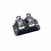
MOSFET N-CH 300V 130A SOT-227B

IXFN130N30

Manufacturer Part Number
IXFN130N30
Description
MOSFET N-CH 300V 130A SOT-227B
Manufacturer
IXYS
Series
HiPerFET™r
Datasheet

Specifications of IXFN130N30

Fet Type
MOSFET N-Channel, Metal Oxide
Fet Feature
Standard
Rds On (max) @ Id, Vgs
22 mOhm @ 500mA, 10V
Drain To Source Voltage (vdss)
300V
Current - Continuous Drain (id) @ 25° C
130A
Vgs(th) (max) @ Id
4V @ 8mA
Gate Charge (qg) @ Vgs
380nC @ 10V
Input Capacitance (ciss) @ Vds
14500pF @ 25V
Power - Max
700W
Mounting Type
Chassis Mount
Package / Case
SOT-227, miniBLOC
Configuration
Single Dual Source
Transistor Polarity
N-Channel
Resistance Drain-source Rds (on)
0.022 Ohms
Forward Transconductance Gfs (max / Min)
92 s
Drain-source Breakdown Voltage
300 V
Gate-source Breakdown Voltage
+/- 20 V
Continuous Drain Current
130 A
Power Dissipation
700 W
Maximum Operating Temperature
+ 150 C
Mounting Style
SMD/SMT
Minimum Operating Temperature
- 55 C
Vdss, Max, (v)
300
Id(cont), Tc=25°c, (a)
130
Rds(on), Max, Tj=25°c, (?)
0.018
Ciss, Typ, (pf)
15500
Qg, Typ, (nc)
555
Trr, Typ, (ns)
-
Trr, Max, (ns)
180
Pd, (w)
694
Rthjc, Max, (ºc/w)
0.18
Package Style
SOT-227B
Lead Free Status / RoHS Status
Lead free / RoHS Compliant

Available stocks

Company
Part Number
Manufacturer
Quantity
Price
Part Number:
IXFN130N30
Manufacturer:
SANKEN
Quantity:
3 000
HiPerFET
Power MOSFETs
Single Die MOSFET
N-Channel Enhancement Mode
Avalanche Rated, High dv/dt, Low t
© 2003 IXYS All rights reserved
Symbol
V
V
V
V
I
I
I
I
E
E
dv/dt
P
T
T
T
V
M
Weight
Symbol
V
V
I
I
R
L(RMS)
DM
AR
D25
GSS
DSS
J
JM
stg
DGR
GS
GSM
AR
AS
D
ISOL
DSS
GH(th)
d
DSS
DS(on)
T
Terminal (current limit)
T
T
T
T
I
T
T
Test Conditions
T
T
Continuous
Transient
50/60 Hz, RMS
I
Mounting torque
Terminal connection torque
S
Test Conditions
V
V
V
V
V
V
Pulse test, t
duty cycle d 2 %
ISOL
C
C
C
C
C
C
J
J
J
GS
DS
GS
DS
GS
GS
= 25 C
= 25 C
= 25 C, pulse width limited by T
= 25 C
= 25 C
= 25 C
= 25 C to 150 C
= 25 C to 150 C; R
= 0 V, I
= V
= 20 V
= V
= 0 V
= 10 V, I
150 C, R
I
TM
DM
1 mA
, di/dt 100 A/ s, V
GS
DSS
, I
D
D
DC
= 3 mA
= 8 mA
D
G
, V
= 0.5 • I
300 s,
= 2
DS
t = 1 min
t = 1 s
= 0
D25
GS
= 1 M
DD
T
T
(T
J
J
rr
J
= 25 C
= 125 C
V
= 25 C, unless otherwise specified)
DSS
JM
,
min.
300
Characteristic Values
IXFN 130N30
2
-55 ... +150
-55 ... +150
Maximum Ratings
typ.
1.5/13 Nm/lb.in.
1.5/13 Nm/lb.in.
2500
3000
S
G
300
300
130
100
520
100
700
150
20
30
85
30
4
5
max.
200
100
22 m
4
2 mA
D
S
V/ns
mJ
V~
V~
nA
W
A
C
C
C
V
V
V
V
A
A
A
g
J
A
V
V
G = Gate
S = Source
Either Source terminal at miniBLOC can be used
as Main or Kelvin Source
miniBLOC, SOT-227 B (IXFN)
Features
Applications
Advantages
International standard packages
miniBLOC, with Aluminium nitride
isolation
Low R
Rugged polysilicon gate cell structure
Unclamped Inductive Switching (UIS)
rated
Low package inductance
Fast intrinsic Rectifier
DC-DC converters
Battery chargers
Switched-mode and resonant-mode
power supplies
DC choppers
Temperature and lighting controls
Easy to mount
Space savings
High power density
E153432
V
I
R
t
D25
DS (on)
rr
DSS
DS(on)
HDMOS
< 250 ns
= 300
= 130
=
D = Drain
G
TM
DS98531F(01/03)
22 m
process
S
D
V
A
S

Related parts for IXFN130N30

IXFN130N30 Summary of contents

Page 1

... GH(th GSS DSS DS DSS 0.5 • I DS(on D25 Pulse test, t 300 s, duty cycle © 2003 IXYS All rights reserved IXFN 130N30 Maximum Ratings 300 = 1 M 300 130 100 520 JM 100 DSS 700 -55 ... +150 150 -55 ... +150 2500 3000 1.5/13 Nm/lb.in. 1.5/13 Nm/lb.in. 30 ...

Page 2

... Pulse test, t 300 s, duty cycle 30A, -di/dt = 100 IXYS reserves the right to change limits, test conditions, and dimensions. IXYS MOSFETS and IGBTs are covered by one or more of the following U.S. patents: Characteristic Values ( unless otherwise specified) J min. typ. max 14500 2650 610 ...

Page 3

... I - Amperes D Figure 3. R normalized to 0.5 I DS(on) vs 150 125 100 -50 - Degrees C C Figure 5. Drain Current vs. Case Temperature © 2003 IXYS All rights reserved V =10V 200 250 value D25 120 75 100 125 150 IXFN 130N30 200 V =10V GS T =125 O C ...

Page 4

... Figure 9. Forward Voltage Drop of the Intrinsic Diode 0.100 0.010 0.001 - Figure 10. Transient Thermal Resistance IXYS reserves the right to change limits, test conditions, and dimensions. IXYS MOSFETS and IGBTs are covered by one or more of the following U.S. patents: 18000 15000 12000 9000 6000 3000 0 400 500 0 Figure 8 ...

Related keywords