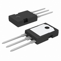
CMF20120D Cree Inc, CMF20120D Datasheet - Page 4

CMF20120D
Manufacturer Part Number
CMF20120D
Description
SIC MOSFET N-CH 1200V TO-247-3
Manufacturer
Cree Inc
Series
SiC MOSFETr
Specifications of CMF20120D
Mfg Application Notes
SiC MOSFETs Application Considerations
Fet Type
SiCFET N-Channel, Silicon Carbide
Fet Feature
Standard
Rds On (max) @ Id, Vgs
110 mOhm @ 20A, 20V
Drain To Source Voltage (vdss)
1200V (1.2kV)
Current - Continuous Drain (id) @ 25° C
33A
Vgs(th) (max) @ Id
4V @ 1mA
Gate Charge (qg) @ Vgs
90.8nC @ 20V
Input Capacitance (ciss) @ Vds
1915pF @ 800V
Power - Max
150W
Mounting Type
Through Hole
Package / Case
TO-247-3
Transistor Polarity
N Channel
Continuous Drain Current Id
33A
Drain Source Voltage Vds
1200V
On Resistance Rds(on)
0.08ohm
Rds(on) Test Voltage Vgs
20V
Configuration
Single
Resistance Drain-source Rds (on)
80 mOhms
Forward Transconductance Gfs (max / Min)
7.3 S, 6.8 S
Drain-source Breakdown Voltage
1200 V
Gate-source Breakdown Voltage
25 V
Continuous Drain Current
33 A
Power Dissipation
150 W
Mounting Style
Through Hole
Gate Charge Qg
90.8 nC
Lead Free Status / RoHS Status
Lead free / RoHS Compliant
Lead Free Status / RoHS Status
Lead free / RoHS Compliant
Applications Information
The Cree SiC MOSFET has removed the upper voltage limit of silicon MOSFETs.
However, there are some differences in characteristics when compared to what is
usually expected with high voltage silicon MOSFETs. These differences need to be
carefully addressed to get maximum benefit from the SiC MOSFET. In general,
although the SiC MOSFET is a superior switch compared to its silicon counterparts,
it should not be considered as a direct drop-in replacement in existing applications.
There are two key characteristics that need to be kept in mind when applying the
SiC MOSFETs: modest transconductance requires that V
needs to be 20 V to
GS
optimize performance. This can be see in the Output and Transfer Characteristics
shown in Figures 1-3. The modest transconductance also affects the transition
where the device behaves as a voltage controlled resistance to where it behaves as
a voltage controlled current source as a funtion of V
The result is that the
DS
.
transition occurs over higher values of V
than are usually experienced with Si
DS
MOSFETs and IGBTs. This might affect the operation anti-desaturation circuits,
especially if the circuit takes advantage of the device entering the constant current
region at low values of forward voltage.
The modest transconductance needs to be carefully considered in the design of the
gate drive circuit. The first obvious requirement is that the gate be capable
of a >22 V (+20 V to -2V) swing. The recommended on state V
is +20 V and the
GS
recommended off state V
is between -2 V to -5 V. Please carefully note that
GS
although the gate voltage swing is higher than the typical silicon MOSFETs and
IGBTs, the total gate charge of the SiC MOSFET is considerably lower. In fact, the
product of gate voltage swing and gate charge for the SiC MOSFET is lower than
comparable silicon devices. The gate voltage must have a fast dV/dt to achieve
fast switching times which indicates that a very low impedance driver is necessary.
Lastly, the fidelity of the gate drive pulse must be carefully controlled. The nominal
2.5V
threshold voltage is 2.5V and the device is not fully on (dV
/dt≈0) until the V
is
DS
GS
above 16V. This is a noticeably wider range than what is typically experienced with
silicon MOSFETs and IGBTs. The net result of this is that the SiC MOSFET has a
somewhat lower ‘noise margin’. Any excessive ringing that is present on the gate
drive signal could cause unintentional turn-on or partial turn-off of the device. The
gate resistance should be carefully selected to ensure that the gate drive pulse is
adequately dampened. To first order, the gate circuit can be approximated as a
simple series RLC circuit driven by a voltage pulse as shown below.
4
CMF20120D Rev. A


