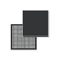
SPEAR300-2 STMicroelectronics, SPEAR300-2 Datasheet - Page 20

SPEAR300-2
Manufacturer Part Number
SPEAR300-2
Description
IC MPU ARM9 289LFBGA
Manufacturer
STMicroelectronics
Series
SPEAr®r
Datasheet
1.SPEAR300-2.pdf
(83 pages)
Specifications of SPEAR300-2
Processor Type
ARM Microprocessor
Speed
333MHz
Voltage
1.14 V ~ 3.6 V
Mounting Type
Surface Mount
Package / Case
289-LFBGA
Processor Series
SPEAr300
Core
ARM926EJ-S
Data Bus Width
16 bit
Maximum Clock Frequency
333 MHz
Operating Supply Voltage
1.2 V
Maximum Operating Temperature
+ 85 C
Mounting Style
SMD/SMT
Data Ram Size
56 KB
Interface Type
I2C, UART, USB, Serial
Number Of Programmable I/os
62
Number Of Timers
6
Program Memory Size
32 KB
Program Memory Type
ROM
Lead Free Status / RoHS Status
Lead free / RoHS Compliant
Features
-
Lead Free Status / Rohs Status
Lead free / RoHS Compliant
Other names
497-10849-5
Available stocks
Company
Part Number
Manufacturer
Quantity
Price
Company:
Part Number:
SPEAR300-2
Manufacturer:
ST
Quantity:
12 005
Part Number:
SPEAR300-2
Manufacturer:
ST
Quantity:
20 000
Architecture overview
2.16
2.17
20/83
SPI_I2C multiple slave control
The SPI interface has only one slave select signal, SS0.
The I
frequently required for CODECs.
The SPI_I2C extension allows management of up to 8 SPI devices, or 8 I
same address (total SPI+I
The SPI extension is made by generating three more slave select signals SS1, SS2 and
SS3.
The I
active.Otherwise the pin remains low, so that the start condition is not met.
Each of the 8 pins can reproduce either the SPI SS0 signal, or the I2C_SCL signal. The
selection is made through a register.
TDM interface
The TDM block implements time division multiplexing.
Main features:
●
●
●
●
●
●
●
●
●
TDM interface with 512 timeslots and up to 16 bufferization channels.
32 ms bufferization for 16 channels (of 4 bytes each)
Supports master and slave mode operation
Programmable clock and synchronization signal generation in master mode
Clock & synchronization signal recovery in slave mode
8 programmable synchronization signals for CODECs
Uses 11 pins:
–
–
–
–
The TDM interface can be the master or a slave of the CLK or SYNC0 signals.
Timeslots can be used for switching or bufferization purposes:
–
–
–
–
2
2
C interface does not allow control of several devices with the same address, which is
C extension is done by replicating the I2C_SCL signal if the corresponding pin is set
SYNC7-0 are dedicated frame syncs for CODECs without timeslot recognition
CLK is the TDM clock
DIN is the TDM input and receives the data
DOUT is the TDM output and transmits the data. It can be high impedance on a
unused timeslot
Switching and bufferization can be used concurrently for different timeslots on the
same TDM
The only limitation is that an output timeslot can not be switched and bufferized at
the same time.
Timeslot switching: any of the output time slots can receive any input timeslot of
the previous frame. The connection memory is part of the action memory,
indicating which timeslot has to be output.
Timeslot bufferization: data from DIN is stored in an input buffer and data from an
output buffer is played on DOUT. When the number of samples stored/played
reaches the buffer size, the processor is interrupted in order to read the input
buffer and prepare a new output buffer (or a DMA request is generated).
2
C devices=8).
Doc ID 16324 Rev 2
2
C devices at the
SPEAr300


