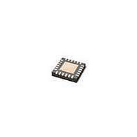
TFA9879HN/N1,157 NXP Semiconductors, TFA9879HN/N1,157 Datasheet - Page 26

TFA9879HN/N1,157
Manufacturer Part Number
TFA9879HN/N1,157
Description
IC AMP AUDIO DGTL MONO D 24HVQFN
Manufacturer
NXP Semiconductors
Type
Class Dr
Datasheet
1.TFA9879HNN1118.pdf
(60 pages)
Specifications of TFA9879HN/N1,157
Output Type
1-Channel (Mono)
Package / Case
24-VFQFN Exposed Pad
Max Output Power X Channels @ Load
2.75W x 1 @ 4 Ohm
Voltage - Supply
2.5 V ~ 5.5 V
Features
Depop, Digital Inputs, I²C, I²S, Mute, Short-Circuit and Thermal Protection, Tone and Volume Control
Mounting Type
Surface Mount
Product
Class-D
Output Power
2.75 W
Thd Plus Noise
0.02 %
Operating Supply Voltage
3.7 V
Supply Current
5.7 mA
Mounting Style
SMD/SMT
Audio - Load Impedance
4 Ohms, 8 Ohms
Audio Load Resistance
4 Ohms, 8 Ohms
Input Signal Type
Serial
Supply Voltage (max)
5.5 V
Supply Voltage (min)
2.5 V
Lead Free Status / RoHS Status
Lead free / RoHS Compliant
NXP Semiconductors
Table 19.
TFA9879
Product data sheet
Start TFA9879
S
address
11011A
I
2
C-bus read cycle
2
A
10.3 I
10.4 Top-level register map
1
R/W
0
The sequence of events that needs to be followed when reading data from the TFA9879’s
I
registers stores two bytes of data. Data is always written in byte pairs. Data transfer is
always MSB first.
The read cycle sequence using SDA is as follows:
10. The microcontroller asserts an acknowledge.
11. The TFA9879 transmits the second byte (the LSB).
12. The microcontroller asserts either an acknowledge or a negative acknowledge (NA).
Table 20
and status areas. There are 21 control registers and 1 status register.
Table 20.
Register address (hex)
00h
01h
02h
03h
04h
05h
2
2
1. The microcontroller asserts a start condition (S).
2. The microcontroller transmits the 7-bit device address of the TFA9879, followed by
3. The TFA9879 asserts an acknowledge (A).
4. The microcontroller transmits the 8-bit TFA9879 register address from which the first
5. The TFA9879 asserts an acknowledge.
6. The microcontroller asserts a repeated start (Sr).
7. The microcontroller re-transmits the device address followed by the R/W bit set to 1.
8. The TFA9879 asserts an acknowledge.
9. The TFA9879 transmits the first byte (the MSB).
C-bus registers is detailed in
C-bus read cycle
A
the R/W bit set to 0.
data byte will be read.
– If the microcontroller asserts an acknowledge, the target register address is
– If the microcontroller asserts a negative acknowledge, the TFA9879 frees the
First
register
address
ADDR
auto-increased by the TFA9879 and steps 9 to 12 are repeated.
I
2
C-bus and the microcontroller generates a stop condition (P).
describes the top-level assignment of register addresses to the functional control
Top-level register map
A
All information provided in this document is subject to legal disclaimers.
Sr
Rev. 02 — 15 October 2010
TFA9879
address
11011A
Default (hex)
0x0000
0x0A18
0x0007
0x0A18
0x0007
0x59DD
2
Table
A
1
Mono BTL class-D audio amplifier with digital input
R/W
1
19. One byte is transmitted at a time. Each of the
R/W
R/W
Access Description
R/W
R/W
R/W
R/W
A
MSB
MS1
device control; see
serial Interface input 1; see
serial Interface input 2; see
equalizer_A word_1; see
PCM/IOM2 format input 1; see
PCM/IOM2 format input 2; see
A
LSB
LS1
A
Table 21
More
data...
<....>
TFA9879
© NXP B.V. 2010. All rights reserved.
Table 24
Table 22
Table 22
NA
Table 23
Table 23
26 of 60
Stop
P


