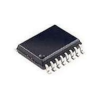
HV9961NG-G Supertex, HV9961NG-G Datasheet - Page 5

HV9961NG-G
Manufacturer Part Number
HV9961NG-G
Description
LED Drivers LED DRIVER WITH AVE RAGE-MODE (I) CNTRL
Manufacturer
Supertex
Datasheet
1.HV9961LG-G.pdf
(9 pages)
Specifications of HV9961NG-G
High Level Output Current
0.165 A
Operating Supply Voltage
8 V to 450 V
Maximum Power Dissipation
1000 mW
Maximum Operating Temperature
+ 125 C
Mounting Style
SMD/SMT
Package / Case
SOIC-16
Minimum Operating Temperature
- 40 C
Operating Supply Voltage (typ)
9/12/15/18/24V
Number Of Segments
1
Operating Temperature (min)
-40C
Operating Temperature (max)
125C
Operating Temperature Classification
Automotive
Package Type
SOIC N
Pin Count
16
Mounting
Surface Mount
Power Dissipation
1W
Lead Free Status / RoHS Status
Lead free / RoHS Compliant
Available stocks
Company
Part Number
Manufacturer
Quantity
Price
Company:
Part Number:
HV9961NG-G
Manufacturer:
Supertex
Quantity:
135
Application Information
General Description
Peak-current control (as in HV9910B) of a buck converter is
the most economical and simple way to regulate its output
current. However, it suffers accuracy and regulation prob-
lems that arise from the so-called peak-to-average current
error, contributed by the current ripple in the output inductor
and the propagation delay in the current sense compara-
tor. The full inductor current signal is unavailable for direct
sensing at the ground potential in a buck converter when
the control switch is referenced to the same ground poten-
tial because the control switch is only conducting for small
periods. While it is very simple to detect the peak current in
the switch, controlling the average inductor current is usu-
ally implemented by level translating the sense signal from
+V
V
sively complex and expensive in the offline AC or other high-
voltage DC applications.
The HV9961 employs Supertex’ proprietary control scheme,
achieving fast and very accurate control of average current
in the buck inductor through sensing the switch current only.
No compensation of the current control loop is required. The
LED current response to PWMD input is similar to that of the
HV9910B. The inductor current ripple amplitude does not af-
fect this control scheme significantly, and therefore, the LED
current is independent of the variation in inductance, switch-
ing frequency or output voltage. Constant off-time control of
the buck converter is used for stability and to improve the
LED current regulation over a wide range of input voltages.
(Note that, unlike HV9910B, the HV9961 does not support
the constant-frequency mode of operation.)
OFF Timer
The timing resistor connected to RT determines the off-time
of the gate driver, and it must be wired to GND. (Wiring this
resistor to GATE as with HV9910B is no longer supported.)
The equation governing the off-time of the GATE output is
given by:
within the range of 30kΩ ≤ R
Average Current Control Feedback and Output
Short Circuit Protection
The current through the switching MOSFET source is aver-
aged and used to give constant-current feedback. This cur-
rent is detected using a sense resistor at the CS pin. The
IN
IN
, this type of average-current control may become exces-
. Though this is practical for relatively low input voltage
T
OFF
(µs) =
Supertex inc.
R
25
T
(kΩ)
+ 0.3
T
≤ 1.0MΩ.
●
1235 Bordeaux Drive, Sunnyvale, CA 94089
(1)
5
feedback operates in a fast open-loop mode. No compensa-
tion is required. Output current is programmed simply as:
when the voltage at the LD input V
The above equations are only valid for continuous conduc-
tion of the output inductor. It is a good practice to design the
inductor such that the switching ripple current in it is 30~40%
of its average peak-to-peak, full load, DC current. Hence,
the recommended inductance can be calculated as:
The duty-cycle range of the current control feedback is lim-
ited to D ≤ 0.75. A reduction in the LED current may occur
when the LED string voltage V
input voltage V
Reducing the output LED voltage V
D
the loss of regulation of the LED current. This condition,
however, causes an increase in the LED current and can
potentially trip the short-circuit protection comparator.
The typical output characteristic of the HV9961 LED driver is
shown in Fig.1. The corresponding HV9910B characteristic
is given for the comparison.
Fig.1. Typical output characteristic of an HV9961 LED
MIN
0.60
0.55
0.50
0.45
0.40
0.35
0.30
0.25
, where D
0
I
I
L
LED
LED
O
●
=
=
=
Tel: 408-222-8888
V
MIN
10
0.275V
IN
O(MAX)
V
R
0.4 • I
of the HV9961 LED driver.
LD
CS
= 1.0µs/(T
Output Characteristics
R
• 0.185
CS
• T
O
20
OFF
Output Voltage (V)
driver.
OFF
●
www.supertex.com
O
30
+1.0µs), may also result in
is greater than 75% of the
LD
O
≥ 1.5V. Otherwise:
below V
40
V
IN
= 170VDC
HV9910B
HV9961
HV9961
O(MIN)
50
= V
(2)
(3)
(4)
IN
60
•


