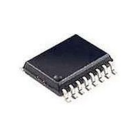
HV9961NG-G Supertex, HV9961NG-G Datasheet - Page 7

HV9961NG-G
Manufacturer Part Number
HV9961NG-G
Description
LED Drivers LED DRIVER WITH AVE RAGE-MODE (I) CNTRL
Manufacturer
Supertex
Datasheet
1.HV9961LG-G.pdf
(9 pages)
Specifications of HV9961NG-G
High Level Output Current
0.165 A
Operating Supply Voltage
8 V to 450 V
Maximum Power Dissipation
1000 mW
Maximum Operating Temperature
+ 125 C
Mounting Style
SMD/SMT
Package / Case
SOIC-16
Minimum Operating Temperature
- 40 C
Operating Supply Voltage (typ)
9/12/15/18/24V
Number Of Segments
1
Operating Temperature (min)
-40C
Operating Temperature (max)
125C
Operating Temperature Classification
Automotive
Package Type
SOIC N
Pin Count
16
Mounting
Surface Mount
Power Dissipation
1W
Lead Free Status / RoHS Status
Lead free / RoHS Compliant
Available stocks
Company
Part Number
Manufacturer
Quantity
Price
Company:
Part Number:
HV9961NG-G
Manufacturer:
Supertex
Quantity:
135
PWM Dimming
Due to the fast open-loop response of the average-current
control loop of the HV9961, its PWM dimming performance
nearly matches that of the HV9910B. The inductor current
waveform comparison is shown in Fig. 4.
Pin Description
Fig.4. Typical PWM dimming response of an HV9961
8-Lead SOIC
[CH2 (red): PWMD; CH4 (green): Inductor Current; CH3 (blue):
1
2
3
4
5
6
7
8
-
Supertex inc.
Same as HV9910B for comparison]
Pin #
16-Lead SOIC
2, 3, 6, 7, 10,
11, 15, 16
LED driver.
12
13
14
1
4
5
8
9
●
Function Description
1235 Bordeaux Drive, Sunnyvale, CA 94089
PWMD
GATE
GND
VDD
VIN
CS
NC
LD
RT
This pin is the input of an 8.0 - 450V linear regulator.
This pin is the current sense pin used to sense the FET current by means
of an external sense resistor.
Ground return for all internal circuitry. This pin must be electrically con-
nected to the ground of the power train.
This pin is the output GATE driver for an external N-channel power
MOSFET.
This is the PWM dimming input of the IC. When this pin is pulled to GND,
the gate driver is turned off. When the pin is pulled high, the gate driver
operates normally.
This is the power supply pin for all internal circuits. It must be bypassed
with a low ESR capacitor to GND (at least 0.1μF).
This pin is the linear dimming input, and it sets the current sense thresh-
old as long as the voltage at this pin is less than 1.5V. If voltage at LD falls
below 150mV, the GATE output is disabled. The GATE signal recovers at
200mV at LD.
A resistor connected between this pin and GND programs the GATE off-
time.
No connection
7
The rising and falling edges are limited by the current slew
rate in the inductor. The first switching cycle is terminated
upon reaching the 275mV (V
cuit is further reaching its steady-state within 3~4 switching
cycles regardless of the switching frequency.
●
Tel: 408-222-8888
●
LD
www.supertex.com
• 0.185) level at CS. The cir-
HV9961


