A000046 Arduino, A000046 Datasheet - Page 122
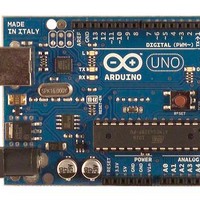
A000046
Manufacturer Part Number
A000046
Description
MCU, MPU & DSP Development Tools Uno
Manufacturer
Arduino
Series
-r
Type
MCUr
Specifications of A000046
Processor To Be Evaluated
ATmega328
Interface Type
USB, I2C, SPI
Dimensions
2.7 in x 2.1 in
Operating Supply Voltage
5 V
Contents
Board
Lead Free Status / RoHS Status
Lead free / RoHS Compliant
For Use With/related Products
ATmega328


15.7
8161D–AVR–10/09
Output Compare Units
cleared by software (writing a logical one to the I/O bit location). For measuring frequency only,
the clearing of the ICF1 Flag is not required (if an interrupt handler is used).
The 16-bit comparator continuously compares TCNT1 with the Output Compare Register
(OCR1x). If TCNT equals OCR1x the comparator signals a match. A match will set the Output
Compare Flag (OCF1x) at the next timer clock cycle. If enabled (OCIE1x = 1), the Output Com-
pare Flag generates an Output Compare interrupt. The OCF1x Flag is automatically cleared
when the interrupt is executed. Alternatively the OCF1x Flag can be cleared by software by writ-
ing a logical one to its I/O bit location. The Waveform Generator uses the match signal to
generate an output according to operating mode set by the Waveform Generation mode
(WGM13:0) bits and Compare Output mode (COM1x1:0) bits. The TOP and BOTTOM signals
are used by the Waveform Generator for handling the special cases of the extreme values in
some modes of operation
A special feature of Output Compare unit A allows it to define the Timer/Counter TOP value (i.e.,
counter resolution). In addition to the counter resolution, the TOP value defines the period time
for waveforms generated by the Waveform Generator.
Figure 15-4
bit names indicates the device number (n = 1 for Timer/Counter 1), and the “x” indicates Output
Compare unit (A/B). The elements of the block diagram that are not directly a part of the Output
Compare unit are gray shaded.
Figure 15-4. Output Compare Unit, Block Diagram
The OCR1x Register is double buffered when using any of the twelve Pulse Width Modulation
(PWM) modes. For the Normal and Clear Timer on Compare (CTC) modes of operation, the
double buffering is disabled. The double buffering synchronizes the update of the OCR1x Com-
pare Register to either TOP or BOTTOM of the counting sequence. The synchronization
shows a block diagram of the Output Compare unit. The small “n” in the register and
OCRnxH Buf. (8-bit)
(See Section “15.9” on page
OCRnxH (8-bit)
BOTTOM
OCRnx Buffer (16-bit Register)
TEMP (8-bit)
TOP
OCRnx (16-bit Register)
ATmega48PA/88PA/168PA/328P
OCRnxL Buf. (8-bit)
OCRnxL (8-bit)
DATA BUS
Waveform Generator
WGMn3:0
=
(16-bit Comparator )
(8-bit)
125.)
COMnx1:0
TCNTnH (8-bit)
OCFnx (Int.Req.)
TCNTn (16-bit Counter)
TCNTnL (8-bit)
OCnx
122
Related parts for A000046
Image
Part Number
Description
Manufacturer
Datasheet
Request
R

Part Number:
Description:
Daughter Cards & OEM Boards ARDUINO UNO PROTO PCB REV 3
Manufacturer:
Arduino
Part Number:
Description:
Daughter Cards & OEM Boards ARDUINO SHIELD PROTO KIT REV 3
Manufacturer:
Arduino
Part Number:
Description:
Daughter Cards & OEM Boards ARDUINO MEGA PROTO KIT REV 3
Manufacturer:
Arduino
Part Number:
Description:
Daughter Cards & OEM Boards ARDUINO MEGA PROTO PCB REV 3
Manufacturer:
Arduino
Part Number:
Description:
Development Boards & Kits - AVR ARDUINO STARTER KIT W/ UNO REV3
Manufacturer:
Arduino
Part Number:
Description:
RF Development Tools ARDUINO SHIELD WIRELESS PROTO
Manufacturer:
Arduino
Datasheet:
Part Number:
Description:
RF Development Tools ARDUINO SHIELD WIRELESS WITH SD
Manufacturer:
Arduino
Datasheet:

Part Number:
Description:
Development Software Getting started w/Arduino
Manufacturer:
Arduino

Part Number:
Description:
Ethernet Modules & Development Tools Ethernet Shield for Arduino
Manufacturer:
Arduino

Part Number:
Description:
MCU, MPU & DSP Development Tools LilyPad Arduino Main Board
Manufacturer:
Arduino

Part Number:
Description:
ARDUINO NANO Board
Manufacturer:
Arduino
Datasheet:
Part Number:
Description:
Ethernet Modules & Development Tools ETHERNET SHEILD PoE FOR ARDUINO
Manufacturer:
Arduino
Datasheet:

Part Number:
Description:
ATMEGA328 MCU IC W/ Arduino UNO Bootloader
Manufacturer:
Arduino
Datasheet:
Part Number:
Description:
Memory Cards MICRO SD CARD 1GB WITH SD ADAPTER
Manufacturer:
Arduino