A000046 Arduino, A000046 Datasheet - Page 275
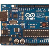
A000046
Manufacturer Part Number
A000046
Description
MCU, MPU & DSP Development Tools Uno
Manufacturer
Arduino
Series
-r
Type
MCUr
Specifications of A000046
Processor To Be Evaluated
ATmega328
Interface Type
USB, I2C, SPI
Dimensions
2.7 in x 2.1 in
Operating Supply Voltage
5 V
Contents
Board
Lead Free Status / RoHS Status
Lead free / RoHS Compliant
For Use With/related Products
ATmega328


25.3
25.3.1
8161D–AVR–10/09
Register Description
SPMCSR – Store Program Memory Control and Status Register
The Store Program Memory Control and Status Register contains the control bits needed to con-
trol the Program memory operations.
• Bit 7 – SPMIE: SPM Interrupt Enable
When the SPMIE bit is written to one, and the I-bit in the Status Register is set (one), the SPM
ready interrupt will be enabled. The SPM ready Interrupt will be executed as long as the SELF-
PRGEN bit in the SPMCSR Register is cleared. The interrupt will not be generated during
EEPROM write or SPM.
• Bit 6 – RWWSB: Read-While-Write Section Busy
This bit is for compatibility with devices supporting Read-While-Write. It will always read as zero
in ATmega48PA.
• Bit 5 – Res: Reserved Bit
This bit is a reserved bit in the ATmega48PA/88PA/168PA/328P and will always read as zero.
• Bit 4 – RWWSRE: Read-While-Write Section Read Enable
T h e f u n c t i o n a l i t y o f t h i s b i t i n A T m e g a 4 8 P A i s a s u b s e t o f t h e f u n c t i o n a l i t y i n
ATmega88PA/168PA. If the RWWSRE bit is written while filling the temporary page buffer, the
temporary page buffer will be cleared and the data will be lost.
• Bit 3 – BLBSET: Boot Lock Bit Set
T h e f u n c t i o n a l i t y o f t h i s b i t i n A T m e g a 4 8 P A i s a s u b s e t o f t h e f u n c t i o n a l i t y i n
ATmega88PA/168PA. An LPM instruction within three cycles after BLBSET and SELFPRGEN
are set in the SPMCSR Register, will read either the Lock bits or the Fuse bits (depending on Z0
in the Z-pointer) into the destination register. See
ware” on page 271
• Bit 2 – PGWRT: Page Write
If this bit is written to one at the same time as SELFPRGEN, the next SPM instruction within four
clock cycles executes Page Write, with the data stored in the temporary buffer. The page
address is taken from the high part of the Z-pointer. The data in R1 and R0 are ignored. The
PGWRT bit will auto-clear upon completion of a Page Write, or if no SPM instruction is executed
within four clock cycles. The CPU is halted during the entire Page Write operation.
• Bit 1 – PGERS: Page Erase
If this bit is written to one at the same time as SELFPRGEN, the next SPM instruction within four
clock cycles executes Page Erase. The page address is taken from the high part of the Z-
pointer. The data in R1 and R0 are ignored. The PGERS bit will auto-clear upon completion of a
Page Erase, or if no SPM instruction is executed within four clock cycles. The CPU is halted dur-
ing the entire Page Write operation.
Bit
0x37 (0x57)
Read/Write
Initial Value
SPMIE
R/W
7
0
for details.
RWWSB
R
6
0
R
5
–
0
ATmega48PA/88PA/168PA/328P
RWWSRE
R/W
4
0
BLBSET
”Reading the Fuse and Lock Bits from Soft-
R/W
3
0
PGWRT
R/W
2
0
PGERS
R/W
1
0
SELFPRGEN
R/W
0
0
SPMCSR
275
Related parts for A000046
Image
Part Number
Description
Manufacturer
Datasheet
Request
R

Part Number:
Description:
Daughter Cards & OEM Boards ARDUINO UNO PROTO PCB REV 3
Manufacturer:
Arduino
Part Number:
Description:
Daughter Cards & OEM Boards ARDUINO SHIELD PROTO KIT REV 3
Manufacturer:
Arduino
Part Number:
Description:
Daughter Cards & OEM Boards ARDUINO MEGA PROTO KIT REV 3
Manufacturer:
Arduino
Part Number:
Description:
Daughter Cards & OEM Boards ARDUINO MEGA PROTO PCB REV 3
Manufacturer:
Arduino
Part Number:
Description:
Development Boards & Kits - AVR ARDUINO STARTER KIT W/ UNO REV3
Manufacturer:
Arduino
Part Number:
Description:
RF Development Tools ARDUINO SHIELD WIRELESS PROTO
Manufacturer:
Arduino
Datasheet:
Part Number:
Description:
RF Development Tools ARDUINO SHIELD WIRELESS WITH SD
Manufacturer:
Arduino
Datasheet:

Part Number:
Description:
Development Software Getting started w/Arduino
Manufacturer:
Arduino

Part Number:
Description:
Ethernet Modules & Development Tools Ethernet Shield for Arduino
Manufacturer:
Arduino

Part Number:
Description:
MCU, MPU & DSP Development Tools LilyPad Arduino Main Board
Manufacturer:
Arduino

Part Number:
Description:
ARDUINO NANO Board
Manufacturer:
Arduino
Datasheet:
Part Number:
Description:
Ethernet Modules & Development Tools ETHERNET SHEILD PoE FOR ARDUINO
Manufacturer:
Arduino
Datasheet:

Part Number:
Description:
ATMEGA328 MCU IC W/ Arduino UNO Bootloader
Manufacturer:
Arduino
Datasheet:
Part Number:
Description:
Memory Cards MICRO SD CARD 1GB WITH SD ADAPTER
Manufacturer:
Arduino