A000046 Arduino, A000046 Datasheet - Page 190
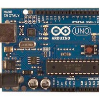
A000046
Manufacturer Part Number
A000046
Description
MCU, MPU & DSP Development Tools Uno
Manufacturer
Arduino
Series
-r
Type
MCUr
Specifications of A000046
Processor To Be Evaluated
ATmega328
Interface Type
USB, I2C, SPI
Dimensions
2.7 in x 2.1 in
Operating Supply Voltage
5 V
Contents
Board
Lead Free Status / RoHS Status
Lead free / RoHS Compliant
For Use With/related Products
ATmega328


19.7.6
19.7.7
19.8
19.8.1
8161D–AVR–10/09
Asynchronous Data Reception
Disabling the Receiver
Flushing the Receive Buffer
Asynchronous Clock Recovery
The UPEn bit is set if the next character that can be read from the receive buffer had a Parity
Error when received and the Parity Checking was enabled at that point (UPMn1 = 1). This bit is
valid until the receive buffer (UDRn) is read.
In contrast to the Transmitter, disabling of the Receiver will be immediate. Data from ongoing
receptions will therefore be lost. When disabled (i.e., the RXENn is set to zero) the Receiver will
no longer override the normal function of the RxDn port pin. The Receiver buffer FIFO will be
flushed when the Receiver is disabled. Remaining data in the buffer will be lost
The receiver buffer FIFO will be flushed when the Receiver is disabled, i.e., the buffer will be
emptied of its contents. Unread data will be lost. If the buffer has to be flushed during normal
operation, due to for instance an error condition, read the UDRn I/O location until the RXCn Flag
is cleared. The following code example shows how to flush the receive buffer.
Note:
The USART includes a clock recovery and a data recovery unit for handling asynchronous data
reception. The clock recovery logic is used for synchronizing the internally generated baud rate
clock to the incoming asynchronous serial frames at the RxDn pin. The data recovery logic sam-
ples and low pass filters each incoming bit, thereby improving the noise immunity of the
Receiver. The asynchronous reception operational range depends on the accuracy of the inter-
nal baud rate clock, the rate of the incoming frames, and the frame size in number of bits.
The clock recovery logic synchronizes internal clock to the incoming serial frames.
illustrates the sampling process of the start bit of an incoming frame. The sample rate is 16 times
the baud rate for Normal mode, and eight times the baud rate for Double Speed mode. The hor-
izontal arrows illustrate the synchronization variation due to the sampling process. Note the
larger time variation when using the Double Speed mode (U2Xn = 1) of operation. Samples
denoted zero are samples done when the RxDn line is idle (i.e., no communication activity).
Assembly Code Example
C Code Example
USART_Flush:
void USART_Flush( void )
{
}
sbis UCSRnA, RXCn
ret
in
rjmp USART_Flush
unsigned char dummy;
while ( UCSRnA & (1<<RXCn) ) dummy = UDRn;
1.
See ”About Code Examples” on page 7.
For I/O Registers located in extended I/O map, “IN”, “OUT”, “SBIS”, “SBIC”, “CBI”, and “SBI”
instructions must be replaced with instructions that allow access to extended I/O. Typically
“LDS” and “STS” combined with “SBRS”, “SBRC”, “SBR”, and “CBR”.
r16, UDRn
(1)
(1)
ATmega48PA/88PA/168PA/328P
Figure 19-5
190
Related parts for A000046
Image
Part Number
Description
Manufacturer
Datasheet
Request
R

Part Number:
Description:
Daughter Cards & OEM Boards ARDUINO UNO PROTO PCB REV 3
Manufacturer:
Arduino
Part Number:
Description:
Daughter Cards & OEM Boards ARDUINO SHIELD PROTO KIT REV 3
Manufacturer:
Arduino
Part Number:
Description:
Daughter Cards & OEM Boards ARDUINO MEGA PROTO KIT REV 3
Manufacturer:
Arduino
Part Number:
Description:
Daughter Cards & OEM Boards ARDUINO MEGA PROTO PCB REV 3
Manufacturer:
Arduino
Part Number:
Description:
Development Boards & Kits - AVR ARDUINO STARTER KIT W/ UNO REV3
Manufacturer:
Arduino
Part Number:
Description:
RF Development Tools ARDUINO SHIELD WIRELESS PROTO
Manufacturer:
Arduino
Datasheet:
Part Number:
Description:
RF Development Tools ARDUINO SHIELD WIRELESS WITH SD
Manufacturer:
Arduino
Datasheet:

Part Number:
Description:
Development Software Getting started w/Arduino
Manufacturer:
Arduino

Part Number:
Description:
Ethernet Modules & Development Tools Ethernet Shield for Arduino
Manufacturer:
Arduino

Part Number:
Description:
MCU, MPU & DSP Development Tools LilyPad Arduino Main Board
Manufacturer:
Arduino

Part Number:
Description:
ARDUINO NANO Board
Manufacturer:
Arduino
Datasheet:
Part Number:
Description:
Ethernet Modules & Development Tools ETHERNET SHEILD PoE FOR ARDUINO
Manufacturer:
Arduino
Datasheet:

Part Number:
Description:
ATMEGA328 MCU IC W/ Arduino UNO Bootloader
Manufacturer:
Arduino
Datasheet:
Part Number:
Description:
Memory Cards MICRO SD CARD 1GB WITH SD ADAPTER
Manufacturer:
Arduino