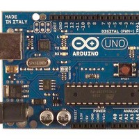
A000046 Arduino, A000046 Datasheet - Page 96
A000046
Manufacturer Part Number
A000046
Description
MCU, MPU & DSP Development Tools Uno
Manufacturer
Arduino
Series
-r
Type
MCUr
Specifications of A000046
Processor To Be Evaluated
ATmega328
Interface Type
USB, I2C, SPI
Dimensions
2.7 in x 2.1 in
Operating Supply Voltage
5 V
Contents
Board
Lead Free Status / RoHS Status
Lead free / RoHS Compliant
For Use With/related Products
ATmega328


14.3
14.4
8161D–AVR–10/09
Timer/Counter Clock Sources
Counter Unit
The Timer/Counter can be clocked internally, via the prescaler, or by an external clock source on
the T0 pin. The Clock Select logic block controls which clock source and edge the Timer/Counter
uses to increment (or decrement) its value. The Timer/Counter is inactive when no clock source
is selected. The output from the Clock Select logic is referred to as the timer clock (clk
The double buffered Output Compare Registers (OCR0A and OCR0B) are compared with the
Timer/Counter value at all times. The result of the compare can be used by the Waveform Gen-
erator to generate a PWM or variable frequency output on the Output Compare pins (OC0A and
OC0B).
Compare Flag (OCF0A or OCF0B) which can be used to generate an Output Compare interrupt
request.
The Timer/Counter can be clocked by an internal or an external clock source. The clock source
is selected by the Clock Select logic which is controlled by the Clock Select (CS02:0) bits
located in the Timer/Counter Control Register (TCCR0B). For details on clock sources and pres-
caler, see
The main part of the 8-bit Timer/Counter is the programmable bi-directional counter unit.
14-2
Figure 14-2. Counter Unit Block Diagram
Signal description (internal signals):
Depending of the mode of operation used, the counter is cleared, incremented, or decremented
at each timer clock (clk
selected by the Clock Select bits (CS02:0). When no clock source is selected (CS02:0 = 0) the
timer is stopped. However, the TCNT0 value can be accessed by the CPU, regardless of
whether clk
count operations.
shows a block diagram of the counter and its surroundings.
count
direction
clear
clk
top
bottom
See Section “15.7.3” on page 123.
Tn
”Timer/Counter0 and Timer/Counter1 Prescalers” on page
T0
is present or not. A CPU write overrides (has priority over) all counter clear or
DATA BUS
TCNTn
T0
). clk
Increment or decrement TCNT0 by 1.
Select between increment and decrement.
Clear TCNT0 (set all bits to zero).
Timer/Counter clock, referred to as clk
Signalize that TCNT0 has reached maximum value.
Signalize that TCNT0 has reached minimum value (zero).
T0
can be generated from an external or internal clock source,
ATmega48PA/88PA/168PA/328P
direction
count
clear
bottom
for details. The compare match event will also set the
Control Logic
top
TOVn
(Int.Req.)
clk
Tn
Clock Select
( From Prescaler )
Detector
Edge
T0
141.
in the following.
Tn
T0
).
Figure
96
Related parts for A000046
Image
Part Number
Description
Manufacturer
Datasheet
Request
R

Part Number:
Description:
Daughter Cards & OEM Boards ARDUINO UNO PROTO PCB REV 3
Manufacturer:
Arduino
Part Number:
Description:
Daughter Cards & OEM Boards ARDUINO SHIELD PROTO KIT REV 3
Manufacturer:
Arduino
Part Number:
Description:
Daughter Cards & OEM Boards ARDUINO MEGA PROTO KIT REV 3
Manufacturer:
Arduino
Part Number:
Description:
Daughter Cards & OEM Boards ARDUINO MEGA PROTO PCB REV 3
Manufacturer:
Arduino
Part Number:
Description:
Development Boards & Kits - AVR ARDUINO STARTER KIT W/ UNO REV3
Manufacturer:
Arduino
Part Number:
Description:
RF Development Tools ARDUINO SHIELD WIRELESS PROTO
Manufacturer:
Arduino
Datasheet:
Part Number:
Description:
RF Development Tools ARDUINO SHIELD WIRELESS WITH SD
Manufacturer:
Arduino
Datasheet:

Part Number:
Description:
Development Software Getting started w/Arduino
Manufacturer:
Arduino

Part Number:
Description:
Ethernet Modules & Development Tools Ethernet Shield for Arduino
Manufacturer:
Arduino

Part Number:
Description:
MCU, MPU & DSP Development Tools LilyPad Arduino Main Board
Manufacturer:
Arduino

Part Number:
Description:
ARDUINO NANO Board
Manufacturer:
Arduino
Datasheet:
Part Number:
Description:
Ethernet Modules & Development Tools ETHERNET SHEILD PoE FOR ARDUINO
Manufacturer:
Arduino
Datasheet:

Part Number:
Description:
ATMEGA328 MCU IC W/ Arduino UNO Bootloader
Manufacturer:
Arduino
Datasheet:
Part Number:
Description:
Memory Cards MICRO SD CARD 1GB WITH SD ADAPTER
Manufacturer:
Arduino