A000046 Arduino, A000046 Datasheet - Page 82
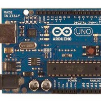
A000046
Manufacturer Part Number
A000046
Description
MCU, MPU & DSP Development Tools Uno
Manufacturer
Arduino
Series
-r
Type
MCUr
Specifications of A000046
Processor To Be Evaluated
ATmega328
Interface Type
USB, I2C, SPI
Dimensions
2.7 in x 2.1 in
Operating Supply Voltage
5 V
Contents
Board
Lead Free Status / RoHS Status
Lead free / RoHS Compliant
For Use With/related Products
ATmega328


13.3.1
8161D–AVR–10/09
Alternate Functions of Port B
The Port B pins with alternate functions are shown in
Table 13-3.
The alternate pin configuration is as follows:
• XTAL2/TOSC2/PCINT7 – Port B, Bit 7
XTAL2: Chip clock Oscillator pin 2. Used as clock pin for crystal Oscillator or Low-frequency
crystal Oscillator. When used as a clock pin, the pin can not be used as an I/O pin.
TOSC2: Timer Oscillator pin 2. Used only if internal calibrated RC Oscillator is selected as chip
clock source, and the asynchronous timer is enabled by the correct setting in ASSR. When the
AS2 bit in ASSR is set (one) and the EXCLK bit is cleared (zero) to enable asynchronous clock-
ing of Timer/Counter2 using the Crystal Oscillator, pin PB7 is disconnected from the port, and
becomes the inverting output of the Oscillator amplifier. In this mode, a crystal Oscillator is con-
nected to this pin, and the pin cannot be used as an I/O pin.
PCINT7: Pin Change Interrupt source 7. The PB7 pin can serve as an external interrupt source.
If PB7 is used as a clock pin, DDB7, PORTB7 and PINB7 will all read 0.
• XTAL1/TOSC1/PCINT6 – Port B, Bit 6
XTAL1: Chip clock Oscillator pin 1. Used for all chip clock sources except internal calibrated RC
Oscillator. When used as a clock pin, the pin can not be used as an I/O pin.
TOSC1: Timer Oscillator pin 1. Used only if internal calibrated RC Oscillator is selected as chip
clock source, and the asynchronous timer is enabled by the correct setting in ASSR. When the
Port Pin
PB7
PB6
PB5
PB4
PB3
PB2
PB1
PB0
Port B Pins Alternate Functions
Alternate Functions
XTAL2 (
TOSC2 (
PCINT7 (Pin Change Interrupt 7)
XTAL1 (
TOSC1 (
PCINT6 (Pin Change Interrupt 6)
SCK (SPI Bus Master clock Input)
PCINT5 (Pin Change Interrupt 5)
MISO (SPI Bus Master Input/Slave Output)
PCINT4 (Pin Change Interrupt 4)
MOSI (SPI Bus Master Output/Slave Input)
OC2A (Timer/Counter2 Output Compare Match A Output)
PCINT3 (Pin Change Interrupt 3)
SS (SPI Bus Master Slave select)
OC1B (Timer/Counter1 Output Compare Match B Output)
PCINT2 (Pin Change Interrupt 2)
OC1A (Timer/Counter1 Output Compare Match A Output)
PCINT1 (Pin Change Interrupt 1)
ICP1 (Timer/Counter1 Input Capture Input)
CLKO (Divided System Clock Output)
PCINT0 (Pin Change Interrupt 0)
Chip Clock Oscillator pin 2
Chip Clock Oscillator pin 1 or External clock input
Timer Oscillator pin 2
Timer Oscillator pin 1
ATmega48PA/88PA/168PA/328P
)
)
)
Table
13-3.
)
82
Related parts for A000046
Image
Part Number
Description
Manufacturer
Datasheet
Request
R

Part Number:
Description:
Daughter Cards & OEM Boards ARDUINO UNO PROTO PCB REV 3
Manufacturer:
Arduino
Part Number:
Description:
Daughter Cards & OEM Boards ARDUINO SHIELD PROTO KIT REV 3
Manufacturer:
Arduino
Part Number:
Description:
Daughter Cards & OEM Boards ARDUINO MEGA PROTO KIT REV 3
Manufacturer:
Arduino
Part Number:
Description:
Daughter Cards & OEM Boards ARDUINO MEGA PROTO PCB REV 3
Manufacturer:
Arduino
Part Number:
Description:
Development Boards & Kits - AVR ARDUINO STARTER KIT W/ UNO REV3
Manufacturer:
Arduino
Part Number:
Description:
RF Development Tools ARDUINO SHIELD WIRELESS PROTO
Manufacturer:
Arduino
Datasheet:
Part Number:
Description:
RF Development Tools ARDUINO SHIELD WIRELESS WITH SD
Manufacturer:
Arduino
Datasheet:

Part Number:
Description:
Development Software Getting started w/Arduino
Manufacturer:
Arduino

Part Number:
Description:
Ethernet Modules & Development Tools Ethernet Shield for Arduino
Manufacturer:
Arduino

Part Number:
Description:
MCU, MPU & DSP Development Tools LilyPad Arduino Main Board
Manufacturer:
Arduino

Part Number:
Description:
ARDUINO NANO Board
Manufacturer:
Arduino
Datasheet:
Part Number:
Description:
Ethernet Modules & Development Tools ETHERNET SHEILD PoE FOR ARDUINO
Manufacturer:
Arduino
Datasheet:

Part Number:
Description:
ATMEGA328 MCU IC W/ Arduino UNO Bootloader
Manufacturer:
Arduino
Datasheet:
Part Number:
Description:
Memory Cards MICRO SD CARD 1GB WITH SD ADAPTER
Manufacturer:
Arduino