TP2540N3-G Supertex, TP2540N3-G Datasheet

MOSFET Small Signal 400V 25Ohm

TP2540N3-G

Manufacturer Part Number
TP2540N3-G
Description
MOSFET Small Signal 400V 25Ohm
Manufacturer
Supertex
Datasheet

Specifications of TP2540N3-G

Minimum Operating Temperature
- 55 C
Configuration
Single
Transistor Polarity
P-Channel
Resistance Drain-source Rds (on)
25 Ohm @ 10 V
Drain-source Breakdown Voltage
400 V
Gate-source Breakdown Voltage
+/- 20 V
Continuous Drain Current
0.086 A
Power Dissipation
740 mW
Maximum Operating Temperature
+ 150 C
Mounting Style
Through Hole
Package / Case
TO-92
Lead Free Status / RoHS Status
Lead free / RoHS Compliant
Features
Applications
-G indicates package is RoHS compliant (‘Green’)
Absolute Maximum Ratings
Absolute Maximum Ratings are those values beyond which damage to the device may
occur. Functional operation under these conditions is not implied. Continuous operation
of the device at the absolute rating level may affect device reliability. All voltages are
referenced to device ground.
*
Supertex inc.
Ordering Information
Parameter
Drain-to-source voltage
Drain-to-gate voltage
Gate-to-source voltage
Operating and storage temperature
Soldering temperature*
Distance of 1.6mm from case for 10 seconds.
Low threshold (-2.4V max.)
High input impedance
Low input capacitance (125pF max.)
Fast switching speeds
Low on-resistance
Free from secondary breakdown
Low input and output leakage
Logic level interfaces - ideal for TTL and CMOS
Solid state relays
Battery operated systems
Photo voltaic drives
Analog switches
General purpose line drivers
Telecom switches
TP2535
Device
Supertex inc.
Package Option
TP2535N3-G
TO-92
1235 Bordeaux Drive, Sunnyvale, CA 94089
P-Channel Enhancement Mode
Vertical DMOS FETs
-55°C to +150°C
+300°C
Value
BV
BV
BV
±20V
DGS
DSS
DSS
-350
(V)
/BV
DGS
General Description
This low threshold enhancement-mode (normally-off)
transistor utilizes a vertical DMOS structure and Supertex’s
well-proven silicon-gate manufacturing process. This
combination produces a device with the power handling
capabilities of bipolar transistors and with the high input
impedance and positive temperature coefficient inherent
in MOS devices. Characteristic of all MOS structures,
this device is free from thermal runaway and thermally-
induced secondary breakdown.
Supertex’s vertical DMOS FETs are ideally suited to a wide
range of switching and amplifying applications where very
low threshold voltage, high breakdown voltage, high input
impedance, low input capacitance, and fast switching
speeds are desired.
Pin Configuration
Product Marking
Package may or may not include the following marks: Si or
Y Y W W
2 5 3 5
R
SiT P
Tel: 408-222-8888
(max)
DS(ON)
(Ω)
25
YY = Year Sealed
WW = Week Sealed
SOURCE
TO-92 (N3)
TO-92 (N3)
V
(max)
www.supertex.com
-2.4
= “Green” Packaging
GS(th)
(V)
DRAIN
GATE
TP2535
I
(min)
-0.4
D(ON)
(A)

Related parts for TP2540N3-G

TP2540N3-G Summary of contents

Page 1

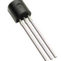
... MOS devices. Characteristic of all MOS structures, this device is free from thermal runaway and thermally- induced secondary breakdown. Supertex’s vertical DMOS FETs are ideally suited to a wide range of switching and amplifying applications where very low threshold voltage, high breakdown voltage, high input impedance, low input capacitance, and fast switching speeds are desired ...

Page 2

... Reverse recovery time rr Notes: 1. All D.C. parameters 100% tested All A.C. parameters sample tested. Switching Waveforms and Test Circuit 0V 10% INPUT -10V t (ON) t d(ON) 0V OUTPUT 10% VDD Supertex inc Power Dissipation (pulsed) O † A (A) (W) -86 -0.6 0. 25°C unless otherwise specified) ...

Page 3

... Typical Performance Curves Supertex inc. ° ° ° ° ● 1235 Bordeaux Drive, Sunnyvale, CA 94089 3 ° ● Tel: 408-222-8888 ● www.supertex.com TP2535 ° ...

Page 4

... 25V DS -1.6 -1.2 -0.8 -0 (volts) GS Capacitance vs. Drain-to-Source Voltage 200 f = 1MHz 150 100 50 C RSS 0 0 -10 -20 V (volts) DS Supertex inc. (cont.) 100 150 -6 -8 -10 C ISS -30 -40 ● 1235 Bordeaux Drive, Sunnyvale, CA 94089 4 On-Resistance vs. Drain Current 100 V = -4. -10V -0.4 -0.8 -1.2 -1 ...

Page 5

... This dimension is not specified in the JEDEC drawing. † This dimension differs from the JEDEC drawing. Drawings not to scale. Supertex Doc.#: DSPD-3TO92N3, Version E041009. (The package drawing(s) in this data sheet may not reflect the most current specifications. For the latest package outline information go to http://www.supertex.com/packaging.html.) does not recommend the use of its products in life support applications, and will not knowingly sell them for use in such applications unless it receives Supertex inc ...

Related keywords