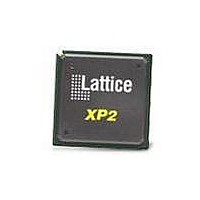
LFXP20C-3FN256C Lattice, LFXP20C-3FN256C Datasheet - Page 353

LFXP20C-3FN256C
Manufacturer Part Number
LFXP20C-3FN256C
Description
FPGA - Field Programmable Gate Array 19.7K LUTS 188 I/O
Manufacturer
Lattice
Specifications of LFXP20C-3FN256C
Number Of Programmable I/os
188
Data Ram Size
405504
Supply Voltage (max)
3.465 V
Maximum Operating Temperature
+ 90 C
Minimum Operating Temperature
0 C
Mounting Style
SMD/SMT
Supply Voltage (min)
1.71 V
Package / Case
FPBGA-256
Lead Free Status / RoHS Status
Lead free / RoHS Compliant
Available stocks
Company
Part Number
Manufacturer
Quantity
Price
Company:
Part Number:
LFXP20C-3FN256C
Manufacturer:
Lattice
Quantity:
135
Company:
Part Number:
LFXP20C-3FN256C
Manufacturer:
Lattice Semiconductor Corporation
Quantity:
10 000
- Current page: 353 of 397
- Download datasheet (10Mb)
Lattice Semiconductor
Figure 17-6. CLOCK_TO_OUT with PLL
Figure 17-7. Trace Report for CLOCK_TO_OUT with PLL
================================================================================
Preference: CLOCK_TO_OUT ALLPORTS 7.000000 ns CLKPORT "ip_macclk" ;
--------------------------------------------------------------------------------
Passed:
IN_DEL
ROUTE
MCLK_DEL
ROUTE
OUTREGF_DE
(100.0% logic, 0.0% route), 1 logic levels.
MCLK_DEL
ROUTE
Report:
Logical Details:
Constraint Details:
Physical Path Details:
Source:
Destination:
Data Path Delay:
Clock Path Delay:
Name
Name
Name
8.249ns delay ip_macclk to rxseln less
5.094ns feedback compensation
3.164ns delay rxseln to rxseln (totaling 6.319ns) meets
7.000ns offset ip_macclk to rxseln by 0.681ns
Clock path ip_macclk to rxseln:
Data path rxseln to rxseln:
Feedback path:
The following path meets requirements by 0.681ns
Fanout
Fanout
Fanout
6.319ns is the minimum offset for this preference.
2 items scored, 0 timing errors detected.
---
---
141
---
---
141
ip_macclk
1
--------
--------
--------
Cell type
IO-FF Out
Port
Delay (ns)
1.192
3.235
0.424
3.398
8.249
Delay (ns)
3.164
Delay (ns)
0.424
3.380
3.804
3.164ns
8.249ns
FBDEL0 = 0.424 ns
ULPPLL.CLKIN to
(19.6% logic, 80.4% route), 2 logic levels.
ULPPLL.CLKIN to
(11.1% logic, 88.9% route), 1 logic levels.
ULPPLL.MCLK to
ULPPLL.MCLK to
FB
CLKI
Pin type
Q
Pad
ULPPL
FBDEL1 = 3.38
CPDEL = 8.25
C17.INDD to
MCLK
(100.0% logic, 0.0% route), 1 logic levels.
(19.6% logic, 80.4% route), 2 logic levels.
C17.PAD to
F32.SC to
ip_macclk_c
Site
Site
Site
Cell name
ppl3_rx5_1_rxselnio
rxseln
17-9
ULPPLL.CLKIN ip_macclk_c
ULPPLL.MCLK v_io_ppl3_tx4_1/mtppll_mac/macpll_0_0
ULPPLL.MCLK v_io_ppl3_tx4_1/mtppll_mac/macpll_0_0
ULPPLL.FB macclk
C17.INDD ip_macclk
F32.PAD rxseln (from macclk)
F32.SC macclk
(clock net +/-)
Resource
Resource
Resource
PIO
DPDEL = 3.17 ns
(from macclk +)
Lattice Semiconductor FPGA
Successful Place and Route
Logic
rxseln
Related parts for LFXP20C-3FN256C
Image
Part Number
Description
Manufacturer
Datasheet
Request
R

Part Number:
Description:
FPGA - Field Programmable Gate Array 19.7K LUTs 340 IO 1. 8/2.5/3.3V -3 Spd I
Manufacturer:
Lattice

Part Number:
Description:
FPGA - Field Programmable Gate Array 19.7K LUTs 268 IO 1. 8/2.5/3.3V -3 Spd
Manufacturer:
Lattice

Part Number:
Description:
FPGA - Field Programmable Gate Array 19.7K LUTs 340 I/O 1.8/2.5/3.3V -3 Spd
Manufacturer:
Lattice
Datasheet:

Part Number:
Description:
FPGA - Field Programmable Gate Array 19.7K LUTs 268 IO 1. 8/2.5/3.3V -3 Spd I
Manufacturer:
Lattice
Part Number:
Description:
FPGA LatticeXP Family 20000 Cells 320MHz 130nm (CMOS) Technology 1.8V/2.5V/3.3V 256-Pin FBGA Tray
Manufacturer:
LATTICE SEMICONDUCTOR
Datasheet:
Part Number:
Description:
FPGA LatticeXP Family 20000 Cells 320MHz 130nm (CMOS) Technology 1.8V/2.5V/3.3V 388-Pin FBGA Tray
Manufacturer:
LATTICE SEMICONDUCTOR
Datasheet:
Part Number:
Description:
FPGA LatticeXP Family 20000 Cells 360MHz 130nm (CMOS) Technology 1.8V/2.5V/3.3V 256-Pin FBGA Tray
Manufacturer:
LATTICE SEMICONDUCTOR
Datasheet:
Part Number:
Description:
FPGA LatticeXP Family 20000 Cells 360MHz 130nm (CMOS) Technology 1.8V/2.5V/3.3V 388-Pin FBGA Tray
Manufacturer:
LATTICE SEMICONDUCTOR
Datasheet:
Part Number:
Description:
FPGA LatticeXP Family 20000 Cells 400MHz 130nm (CMOS) Technology 1.8V/2.5V/3.3V 256-Pin FBGA Tray
Manufacturer:
LATTICE SEMICONDUCTOR
Datasheet:
Part Number:
Description:
FPGA LatticeXP Family 20000 Cells 400MHz 130nm (CMOS) Technology 1.8V/2.5V/3.3V 256-Pin FBGA Tray
Manufacturer:
LATTICE SEMICONDUCTOR
Datasheet:

Part Number:
Description:
IC FPGA 19.7KLUTS 188I/O 256-BGA
Manufacturer:
Lattice
Datasheet:

Part Number:
Description:
IC FPGA 19.7KLUTS 340I/O 484-BGA
Manufacturer:
Lattice
Datasheet:

Part Number:
Description:
IC FPGA 19.7KLUTS 188I/O 256-BGA
Manufacturer:
Lattice
Datasheet:

Part Number:
Description:
IC FPGA 19.7KLUTS 188I/O 256-BGA
Manufacturer:
Lattice
Datasheet:


