IP3088CX10,135 NXP Semiconductors, IP3088CX10,135 Datasheet
IP3088CX10,135
Specifications of IP3088CX10,135


Related parts for IP3088CX10,135


IP3088CX10,135 Summary of contents
Page 1
IP3088CX5; IP3088CX10; IP3088CX15; IP3088CX20 Integrated and 8-channel passive LC-filter network with ESD protection to IEC 61000-4-2 level 4 Rev. 01 — 12 February 2010 1. Product profile 1.1 General description IP3088CX5, IP3088CX10, IP3088CX15 and IP3088CX20 is a ...
Page 2
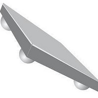
... NXP Semiconductors 2. Pinning information 2.1 Pinning bump A1 index area 001aak061 transparent top view, solder balls facing down Fig 1. Pin configuration IP3088CX5 bump A1 index area transparent top view, solder balls facing down Fig 3. Pin configuration IP3088CX15 2.2 Pin description Table 1. Pinning Pin ...
Page 3
... NXP Semiconductors 3. Ordering information Table 2. Ordering information Type number Package Name IP3088CX5 WLCSP5 IP3088CX10 WLCSP10 IP3088CX15 WLCSP15 IP3088CX20 WLCSP20 4. Functional diagram Fig 5. Schematic diagram IP3088CX5; IP3088CX10; IP3088CX15; IP3088CX20 5. Limiting values Table 3. Limiting values In accordance with the Absolute Maximum Rating System (IEC 60134). ...
Page 4
... NXP Semiconductors 6. Characteristics Table amb Symbol Parameter R s(ch) L s(ch [1] Guaranteed by design. Table amb Symbol Parameter α −3dB 7. Application information 7.1 Insertion loss IP3088CX5, IP3088CX10, IP3088CX15 and IP3088CX20 is mainly designed as an ElectroMagnetic Interference (EMI) and Radio Frequency Interference (RFI) filter for Subscriber Identity Module (SIM) card interfaces. ...
Page 5
... NXP Semiconductors As an example, the measured insertion loss magnitude for all channels of the IP3088CX10 are shown (dB) −10 −20 −30 −40 − Channel 1 (pins A1 and C1 (dB) −10 −20 −30 −40 − Channel 3 (pins A3 and C3) Fig 7. Measured insertion loss magnitude IP3088CX5_CX10_CX15_CX20_1 Product data sheet ...
Page 6
... NXP Semiconductors 8. Package outline WLCSP20: wafer level chip-size package; 20 bumps (8-4-8) bump A1 index area European projection Fig 8. Package outline IP3088CX20 (WLCSP20) Table 6. Dimensions for Figure 8 Symbol IP3088CX5_CX10_CX15_CX20_1 Product data sheet IP3088CX5/CX10/CX15/CX20 and 8-channel passive LC-filter network with ESD protection D 1 Min Typ 0 ...
Page 7
... NXP Semiconductors WLCSP15: wafer level chip-size package; 15 bumps (6-3-6) bump A1 index area European projection Fig 9. Package outline IP3088CX15 (WLCSP15) Table 7. Dimensions for Figure 9 Symbol IP3088CX5_CX10_CX15_CX20_1 Product data sheet IP3088CX5/CX10/CX15/CX20 and 8-channel passive LC-filter network with ESD protection D 1 Min Typ 0.60 ...
Page 8
... NXP Semiconductors WLCSP10: wafer level chip-size package; 10 bumps (4-2-4) bump A1 index area European projection Fig 10. Package outline IP3088CX10 (WLCSP10) Table 8. Dimensions for Figure 10 Symbol IP3088CX5_CX10_CX15_CX20_1 Product data sheet IP3088CX5/CX10/CX15/CX20 and 8-channel passive LC-filter network with ESD protection 1/2 e Min Typ 0.60 ...
Page 9
... NXP Semiconductors WLCSP5: wafer level chip-size package; 5 bumps (2-1-2) bump A1 index area 1 European projection Fig 11. Package outline IP3088CX5 (WLCSP5) Table 9. Dimensions for Figure 11 Symbol IP3088CX5_CX10_CX15_CX20_1 Product data sheet IP3088CX5/CX10/CX15/CX20 and 8-channel passive LC-filter network with ESD protection Min Typ 0.60 0.65 ...
Page 10
... NXP Semiconductors 9. Soldering of WLCSP packages 9.1 Introduction to soldering WLCSP packages This text provides a very brief insight into a complex technology. A more in-depth account of soldering WLCSP (Wafer Level Chip-Size Packages) can be found in application note AN10439 “Wafer Level Chip Scale Package” and in application note AN10365 “Surface mount reflow soldering description” ...
Page 11
... NXP Semiconductors Fig 12. Temperature profiles for large and small components For further information on temperature profiles, refer to application note AN10365 “Surface mount reflow soldering description”. 9.3.1 Stand off The stand off between the substrate and the chip is determined by: • The amount of printed solder on the substrate • ...
Page 12
... NXP Semiconductors Device removal can be done when the substrate is heated until it is certain that all solder joints are molten. The chip can then be carefully removed from the substrate without damaging the tracks and solder lands on the substrate. Removing the device must be done using plastic tweezers, because metal tweezers can damage the silicon ...
Page 13
... Terms and conditions of commercial sale of NXP Semiconductors. Right to make changes — NXP Semiconductors reserves the right to make changes to information published in this document, including without limitation specifications and product descriptions, at any time and without notice ...
Page 14
... NXP Semiconductors’ specifications such use shall be solely at customer’s own risk, and (c) customer fully indemnifies NXP Semiconductors for any liability, damages or failed product claims resulting from customer design and use of the product for automotive applications beyond NXP Semiconductors’ ...
Page 15
... NXP Semiconductors 14. Contents 1 Product profile . . . . . . . . . . . . . . . . . . . . . . . . . . 1 1.1 General description . . . . . . . . . . . . . . . . . . . . . 1 1.2 Features and benefits . . . . . . . . . . . . . . . . . . . . 1 1.3 Applications . . . . . . . . . . . . . . . . . . . . . . . . . . . 1 2 Pinning information . . . . . . . . . . . . . . . . . . . . . . 2 2.1 Pinning . . . . . . . . . . . . . . . . . . . . . . . . . . . . . . . 2 2.2 Pin description . . . . . . . . . . . . . . . . . . . . . . . . . 2 3 Ordering information . . . . . . . . . . . . . . . . . . . . . 3 4 Functional diagram . . . . . . . . . . . . . . . . . . . . . . 3 5 Limiting values Characteristics . . . . . . . . . . . . . . . . . . . . . . . . . . 4 7 Application information 7.1 Insertion loss . . . . . . . . . . . . . . . . . . . . . . . . . . 4 8 Package outline . . . . . . . . . . . . . . . . . . . . . . . . . 6 9 Soldering of WLCSP packages ...