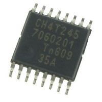
74AVCH4T245PW,118 NXP Semiconductors, 74AVCH4T245PW,118 Datasheet - Page 7

74AVCH4T245PW,118
Manufacturer Part Number
74AVCH4T245PW,118
Description
TXRX 4BIT TRANSLATING 16TSSOP
Manufacturer
NXP Semiconductors
Datasheet
1.74AVCH4T245PW118.pdf
(29 pages)
Specifications of 74AVCH4T245PW,118
Logic Family
74ACH
Number Of Channels Per Chip
2
Propagation Delay Time
6 ns, 12 ns
Supply Voltage (max)
3.6 V
Supply Voltage (min)
0.8 V
Maximum Operating Temperature
+ 125 C
Package / Case
TSSOP-16
Maximum Power Dissipation
500 mW
Minimum Operating Temperature
- 40 C
Mounting Style
SMD/SMT
Lead Free Status / RoHS Status
Lead free / RoHS Compliant
Other names
568-5259-2
NXP Semiconductors
10. Static characteristics
Table 7.
At recommended operating conditions; voltages are referenced to GND (ground = 0 V).
[1]
[2]
[3]
[4]
[5]
[6]
[7]
74AVCH4T245
Product data sheet
Symbol Parameter
V
V
I
I
I
I
I
I
I
C
C
I
BHL
BHH
BHLO
BHHO
OZ
OFF
OH
OL
I
I/O
V
V
The bus hold circuit can sink at least the minimum low sustaining current at V
and then raising it to V
The bus hold circuit can source at least the minimum high sustaining current at V
and then lowering it to V
An external driver must source at least I
An external driver must sink at least I
For I/O ports, the parameter I
CCO
CCI
is the supply voltage associated with the data input port.
is the supply voltage associated with the output port.
HIGH-level output voltage
LOW-level output voltage
input leakage current
bus hold LOW current
bus hold HIGH current
bus hold LOW overdrive
current
bus hold HIGH overdrive
current
OFF-state output current
power-off leakage current
input capacitance
input/output capacitance
Typical static characteristics at T
IL
IH
max.
min.
OZ
includes the input leakage current.
BHHO
Conditions
V
V
nDIR, nOE input; V
V
A or B port; V
A or B port; V
A or B port; V
A or B port; V
A or B port; V
V
suspend mode A port; V
V
suspend mode B port; V
V
A port; V
V
B port; V
V
nDIR, nOE input; V
V
A and B port; V
V
BHLO
I
I
CC(A)
CC(A)
CC(A)
CC(A)
CC(A)
CC(B)
CC(A)
CC(A)
I
I
= V
= V
O
O
to switch this node from HIGH to LOW.
All information provided in this document is subject to legal disclaimers.
= 1.5 mA; V
= 1.5 mA; V
to switch this node from LOW to HIGH.
IH
IH
= V
= V
= 3.6 V; V
= 0 V; V
= 0 V; V
= 0 V; V
= V
= V
amb
or V
or V
I
I
or V
or V
CC(B)
CC(B)
CC(B)
CC(B)
Rev. 2 — 3 December 2010
= 25 C
IL
IL
I
I
CC(A)
CC(A)
O
O
O
= 0.42 V; V
= 0.78 V; V
CC(B)
CC(B)
CC(A)
O
= 0.8 V to 3.6 V
= 0 V or V
= 3.6 V
= 3.3 V
= 3.3 V
= 0 V to 3.6 V;
= 0 V to 3.6 V;
CC(A)
CC(B)
= 3.3 V or 0 V;
CC(A)
= V
= V
I
I
[1][2]
= 3.6 V
= 0.8 V to 3.6 V
= 0.8 V to 3.6 V
= 0 V or 3.6 V;
= 0 V or 3.3 V;
= V
= 0 V
CC(B)
CC(B)
= V
O
O
CC(B)
CCO
CC(A)
CC(A)
= 0 V or V
= 0 V or V
CC(B)
= 1.2 V
= 1.2 V
4-bit dual supply translating transceiver; 3-state
;
= 0.8 V
= V
= V
= 0.8 V
IL
CC(B)
CC(B)
max. I
CCO
CCO
IH
min. I
= 1.2 V
= 1.2 V
;
;
BHL
BHH
should be measured after lowering V
should be measured after raising V
74AVCH4T245
[3]
[4]
[5]
[6]
[7]
[7]
[7]
Min
-
-
-
-
-
-
-
-
-
-
-
-
-
-
Typ
0.69
0.07
0.025 0.25 A
26
24
27
26
0.5
0.5
0.5
0.1
0.1
1.0
4.0
© NXP B.V. 2010. All rights reserved.
Max
-
-
-
-
-
-
2.5
2.5
2.5
1
1
-
-
I
to GND
I
7 of 29
to V
Unit
V
V
A
A
A
A
A
A
A
A
A
pF
pF
CC


