140-0000-973 Emerson Network Power, 140-0000-973 Datasheet - Page 8
140-0000-973
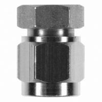
Manufacturer Part Number
140-0000-973
Description
CONN JACK SMA END LAUNCH FIXTURE
Manufacturer
Emerson Network Power
Series
SMAr
Specifications of 140-0000-973
Accessory Type
End Launch Connector
Product
Crimping, Stripping & Cutting Tools & Drills
Description/function
Soldering Mating Fixture for SMA Jacks
For Use With/related Products
SMA Jacks
Lead Free Status / RoHS Status
Not applicable / Not applicable
Lead Free Status / RoHS Status
Not applicable / Not applicable, Lead free / RoHS Compliant
Other names
J10081


Mounting Footprint Info
1. All of the drilled holes are plated through the entire circuit board stackup.
2. All hole patterns are symmetrical about center of the trace.
3. The recommended mounting footprints are shown for the top (signal) side of the board only. Use ground planes on additional layers where
4. For optimum high frequency circuit board performance, use the following fabrication guidelines:
* These calculated dimensions assume a quasi-static mode of propagation, but dispersion does exist for coplanar waveguide. The characteris-
tic impedance and effective dielectric constant may increase slightly for X-band and higher frequencies, unless very small ground to ground
gap spacing is used.
It is assumed the conductors have rectangular cross-sections. The etching process used in circuit board fabrication actually produces trape-
zoidal shapes. Therefore, the GCPW impedance may increase somewhere between that of a perfect rectangular conductor and a theoretical
zero thickness conductor.
High Frequency SMA End Launch Connectors
Mounting Instructions
8
appropriate.
Part Number
142-0761-801
142-0761-811
142-0761-821
142-0761-831
142-0761-841
142-0761-851
142-0761-861
142-0761-871
142-0761-881
142-0761-891
142-0771-821
142-0771-831
Figure 1
A. Maintain a solid ground plane below the high frequency substrate layer.
B. Control the pullback of the trace and grounds from the board edge.
C. Continue the grounded coplanar waveguide line beyond the ground pad area.
D. Place 16 mil diameter ground vias on both sides of the coplanar waveguide line, spaced at 50 mil intervals along the entire length of
E. Immersion gold plate (ENIG) all high frequency conductors per IPC-4552.
F. Do not coat the coplanar waveguide signal trace or open ground gaps with soldermask.
the line.
Emerson Network Power • Tel: 800.247.8256 • Fax 507.833.6287 • www.EmersonNetworkPower.com/connectivity
.0080 (0.203)
.0080 (0.203)
.0160 (0.406)
.0160 (0.406)
.0080 (0.203)
.0080 (0.203)
.0160 (0.406)
.0160 (0.406)
.0080 (0.203)
.0080 (0.203)
.0160 (0.406)
.0160 (0.406)
Thickness
Substrate
Reference dimensions for 50 ohm grounded coplanar waveguide using
Rogers Corporation RO4003C™ high frequency substrate laminate *
GCPW 50Ω Impedance Reference Dimensions *
.0014 (0.036)
.0014 (0.036)
.0014 (0.036)
.0014 (0.036)
.0014 (0.036)
.0014 (0.036)
.0014 (0.036)
.0014 (0.036)
.0014 (0.036)
.0014 (0.036)
.0014 (0.036)
.0014 (0.036)
Conductor
Thickness
Trace Width “A”
.0155 (0.394)
.0155 (0.394)
.0285 (0.724)
.0285 (0.724)
.0155 (0.394)
.0155 (0.394)
.0285 (0.724)
.0285 (0.724)
.0155 (0.394)
.0155 (0.394)
.0285 (0.724)
.0285 (0.724)
Figure 2
Ground Gaps
.0100 (0.254)
.0100 (0.254)
.0100 (0.254)
.0100 (0.254)
.0100 (0.254)
.0100 (0.254)
.0100 (0.254)
.0100 (0.254)
.0100 (0.254)
.0100 (0.254)
.0100 (0.254)
.0100 (0.254)
“B”
Fig
1
1
1
1
2
2
2
2
1
2
1
2
Mounting and Via Holes
.066 (1.68)
.066 (1.68)
.084 (2.13)
.084 (2.13)
.066 (1.68)
.066 (1.68)
.084 (2.13)
.084 (2.13)
.066 (1.68)
.066 (1.68)
.084 (2.13)
.084 (2.13)
“C”
.096 (2.44)
.096 (2.44)
.113 (2.87)
.113 (2.87)
.096 (2.44)
.113 (2.87)
“D”
Related parts for 140-0000-973
Image
Part Number
Description
Manufacturer
Datasheet
Request
R

Part Number:
Description:
TRANSDUCERS SPECTROL / 140-0-0 50 OHM 1 SECT
Manufacturer:
Vishay

Part Number:
Description:
POT 2.0K OHM WW SINGLE TURN
Manufacturer:
Vishay
Datasheet:

Part Number:
Description:
POT 10K OHM WW SINGLE TURN
Manufacturer:
Vishay
Datasheet:

Part Number:
Description:
POT 1.0K OHM WW SINGLE TURN
Manufacturer:
Vishay
Datasheet:

Part Number:
Description:
POT 5.0K OHM WW SINGLE TURN
Manufacturer:
Vishay
Datasheet:

Part Number:
Description:
AC/DC Front end 12Vo 36A 12Vsb Standard Airflow
Manufacturer:
Emerson Network Power

Part Number:
Description:
POWER SUPPLY DIN 24VDC 10A
Manufacturer:
Emerson Network Power
Datasheet:

Part Number:
Description:
POWER SUPPLY SGL 48VOUT 40W 3X5"
Manufacturer:
Emerson Network Power
Datasheet:

Part Number:
Description:
POWER SUP MED&ITE 48V 45W 2"X4"
Manufacturer:
Emerson Network Power
Datasheet:

Part Number:
Description:
POWER SUPPLY 60W 12V OUT
Manufacturer:
Emerson Network Power
Datasheet:

Part Number:
Description:
POWER SUPPLY 60W 48V OUT
Manufacturer:
Emerson Network Power
Datasheet:

Part Number:
Description:
POWER SUPPLY 60W 15V OUT
Manufacturer:
Emerson Network Power
Datasheet:

Part Number:
Description:
POWER SUPPLY TRPL 3.3/5/12V 40W
Manufacturer:
Emerson Network Power
Datasheet:

Part Number:
Description:
POWER SUPPLY SWITCHER 24V 40W
Manufacturer:
Emerson Network Power
Datasheet:

Part Number:
Description:
Linear & Switching Power Supplies 24V output 25W 2A Medical &Non-Medical
Manufacturer:
Emerson Network Power
Datasheet: