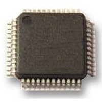
PCA9626B NXP Semiconductors, PCA9626B Datasheet - Page 38

PCA9626B
Manufacturer Part Number
PCA9626B
Description
IC, LED DRIVER, RGBA, 48-LQFP
Manufacturer
NXP Semiconductors
Datasheet
1.PCA9626B118.pdf
(47 pages)
Specifications of PCA9626B
No. Of Outputs
24
Output Current
100mA
Output Voltage
40V
Input Voltage
2.3V To 5.5V
Dimming Control Type
PWM
Driver Case Style
LQFP
Switching Frequency
1MHz
Base Number
9626
Operating
RoHS Compliant
Led Driver Application
RGB Or RGBA LED Drivers, LED Status Information, Displays, Backlights
Rohs Compliant
Yes
Lead Free Status / Rohs Status
Details
Available stocks
Company
Part Number
Manufacturer
Quantity
Price
Part Number:
PCA9626B
Manufacturer:
NXP/恩智浦
Quantity:
20 000
Company:
Part Number:
PCA9626B,118
Manufacturer:
NXP Semiconductors
Quantity:
10 000
Part Number:
PCA9626B,118
Manufacturer:
NXP/恩智浦
Quantity:
20 000
Company:
Part Number:
PCA9626B/S911
Manufacturer:
FREESCALE
Quantity:
430
Part Number:
PCA9626BS
Manufacturer:
NXP/恩智浦
Quantity:
20 000
Company:
Part Number:
PCA9626BЈ¬118
Manufacturer:
PH3
Quantity:
90
NXP Semiconductors
Table 19.
[1]
[2]
[3]
[4]
[5]
[6]
PCA9626_2
Product data sheet
Symbol Parameter
Output port timing
t
t
d(SCL-Q)
d(SDA-Q)
Fig 18. Definition of timing
t
t
A master device must internally provide a hold time of at least 300 ns for the SDA signal (refer to the V
bridge the undefined region of SCL’s falling edge.
The maximum t
250 ns. This allows series protection resistors to be connected between the SDA and the SCL pins and the SDA/SCL bus lines without
exceeding the maximum specified t
C
Input filters on the SDA and SCL inputs suppress noise spikes less than 50 ns.
VD;ACK
VD;DAT
b
SDA
SCL
= total capacitance of one bus line in pF.
= minimum time for SDA data out to be valid following SCL LOW.
delay time from SCL
to data output
delay time from SDA
to data output
= time for Acknowledgement signal from SCL LOW to SDA (out) LOW.
Dynamic characteristics
P
t
BUF
f
for the SDA and SCL bus lines is specified at 300 ns. The maximum fall time (t
S
t
HD;STA
t
LOW
Conditions
SCL to LEDn;
MODE2[3] = 1;
outputs change on
ACK
SDA to LEDn;
MODE2[3] = 0;
outputs change on
STOP condition
f
.
…continued
t
t
r
HD;DAT
Rev. 02 — 31 August 2009
t
HIGH
t
f
t
SU;DAT
Standard-mod
Min
e I
-
-
2
C-bus
24-bit Fm+ I
Max
-
-
Sr
t
SU;STA
Fast-mode
Min
t
HD;STA
I
-
-
2
2
f
C-bus
C-bus 100 mA 40 V LED driver
) for the SDA output stage is specified at
IL
Max
of the SCL signal) in order to
-
-
t
SP
t
SU;STO
PCA9626
Plus I
Min
Fast-mode
© NXP B.V. 2009. All rights reserved.
-
-
2
C-bus
002aaa986
Max
450
450
P
38 of 47
Unit
ns
ns


