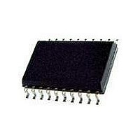
PCA9634PW NXP Semiconductors, PCA9634PW Datasheet - Page 12

PCA9634PW
Manufacturer Part Number
PCA9634PW
Description
IC, LED DRIVER, RGBA, 20-TSSOP
Manufacturer
NXP Semiconductors
Datasheet
1.PCA9634D112.pdf
(38 pages)
Specifications of PCA9634PW
No. Of Outputs
8
Output Current
25mA
Output Voltage
5.5V
Input Voltage
2.3V To 5.5V
Dimming Control Type
PWM
Driver Case Style
TSSOP
Switching Frequency
1MHz
Base Number
9634
Operating
RoHS Compliant
Number Of Segments
16
Low Level Output Current
200 mA
High Level Output Current
50 uA
Operating Supply Voltage
2.3 V to 5.5 V
Maximum Supply Current
10 mA
Maximum Power Dissipation
400 mW
Maximum Operating Temperature
+ 85 C
Mounting Style
SMD/SMT
Package / Case
TSSOP-20
Minimum Operating Temperature
- 40 C
Led Driver Application
RGB Or RGBA LED Drivers, LED Status Information, Displays, Backlights
Rohs Compliant
Yes
Lead Free Status / Rohs Status
Details
Available stocks
Company
Part Number
Manufacturer
Quantity
Price
Company:
Part Number:
PCA9634PW
Manufacturer:
TRINAMIC
Quantity:
1 200
Company:
Part Number:
PCA9634PW
Manufacturer:
NXP Semiconductors
Quantity:
26 963
Part Number:
PCA9634PW
Manufacturer:
NXP/恩智浦
Quantity:
20 000
NXP Semiconductors
Table 6.
Legend: * default value.
[1]
[2]
[3]
PCA9634_6
Product data sheet
Bit
1 to 0
See
mode. Some newer LEDs include integrated Zener diodes to limit voltage transients, reduce EMI and protect the LEDs, and these must
be driven only in the open-drain mode to prevent overheating the IC.
Change of the outputs at the STOP command allows synchronizing outputs of more than one PCA9634. Applicable to registers from
02h (PWM0) to 0Dh (LEDOUT) only.
See
Section 7.7 “Using the PCA9634 with and without external drivers”
Section 7.4 “Active LOW output enable input”
Symbol
OUTNE[1:0]
MODE2 - Mode register 2 (address 01h) bit description
7.3.3 PWM0 to PWM7: Individual brightness control
[3]
Table 7.
Legend: * default value.
A 97 kHz fixed frequency signal is used for each output. Duty cycle is controlled through
256 linear steps from 00h (0 % duty cycle = LED output off) to FFh
(99.6 % duty cycle = LED output at maximum brightness). Applicable to LED outputs
programmed with LDRx = 10 or 11 (LEDOUT0 and LEDOUT1 registers).
duty cycle
Access
R/W
Address
02h
03h
04h
05h
06h
07h
08h
09h
Register
PWM0
PWM1
PWM2
PWM3
PWM4
PWM5
PWM6
PWM7
PWM0 to PWM7 - PWM registers 0 to 7 (address 02h to 09h) bit description
=
Value
00
01*
10
11
------------------------
IDC 7:0
256
Description
when OE = 1 (output drivers not enabled), LEDn = 0
when OE = 1 (output drivers not enabled):
when OE = 1 (output drivers not enabled), LEDn = high-impedance
reserved
Rev. 06 — 12 September 2008
for more details.
Bit
7:0
7:0
7:0
7:0
7:0
7:0
7:0
7:0
LEDn = 1 when OUTDRV = 1
LEDn = high-impedance when OUTDRV = 0 (same as OUTNE[1:0] = 10)
Symbol
IDC0[7:0]
IDC1[7:0]
IDC2[7:0]
IDC3[7:0]
IDC4[7:0]
IDC5[7:0]
IDC6[7:0]
IDC7[7:0]
for more details. Normal LEDs can be driven directly in either
Access Value
R/W
R/W
R/W
R/W
R/W
R/W
R/W
R/W
…continued
0000 0000* PWM0 Individual Duty Cycle
0000 0000* PWM1 Individual Duty Cycle
0000 0000* PWM2 Individual Duty Cycle
0000 0000* PWM3 Individual Duty Cycle
0000 0000* PWM4 Individual Duty Cycle
0000 0000* PWM5 Individual Duty Cycle
0000 0000* PWM6 Individual Duty Cycle
0000 0000* PWM7 Individual Duty Cycle
8-bit Fm+ I
Description
PCA9634
2
© NXP B.V. 2008. All rights reserved.
C-bus LED driver
12 of 38
(1)


