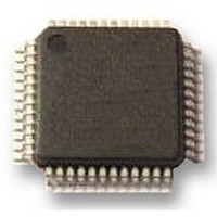
SC16C752BIB48 NXP Semiconductors, SC16C752BIB48 Datasheet - Page 5

SC16C752BIB48
Manufacturer Part Number
SC16C752BIB48
Description
IC, UART, DUAL, 64BYTE FIFO, 16C752
Manufacturer
NXP Semiconductors
Datasheet
1.SC16C752BIBS128.pdf
(47 pages)
Specifications of SC16C752BIB48
No. Of Channels
2
Data Rate
5Mbps
Supply Voltage Range
2.25V To 5.5V
Operating Temperature Range
-40°C To +85°C
Digital Ic Case Style
LQFP
No. Of Pins
48
Svhc
No SVHC (18-Jun-2010)
Uart Features
DMA Signalling Capability, Software Selectable Baud Rate Generator
Rohs Compliant
Yes
Lead Free Status / RoHS Status
Lead free / RoHS Compliant
Available stocks
Company
Part Number
Manufacturer
Quantity
Price
Company:
Part Number:
SC16C752BIB48
Manufacturer:
NXP Semiconductors
Quantity:
1 940
Company:
Part Number:
SC16C752BIB48
Manufacturer:
TI
Quantity:
430
Part Number:
SC16C752BIB48
Manufacturer:
NXP/恩智浦
Quantity:
20 000
Company:
Part Number:
SC16C752BIB48,128
Manufacturer:
NXP Semiconductors
Quantity:
10 000
Company:
Part Number:
SC16C752BIB48,151
Manufacturer:
NXP Semiconductors
Quantity:
10 000
Company:
Part Number:
SC16C752BIB48,157
Manufacturer:
NXP Semiconductors
Quantity:
10 000
NXP Semiconductors
Table 2.
SC16C752B
Product data sheet
Symbol
A0
A1
A2
CDA
CDB
CSA
CSB
CTSA
CTSB
D0
D1
D2
D3
D4
D5
D6
D7
DSRA
DSRB
DTRA
DTRB
GND
INTA
INTB
IOR
Pin description
26
30
29
Pin
LQFP48 HVQFN32
28
27
40
16
10
11
38
23
44
45
46
47
48
1
2
3
39
20
34
35
17
19
5.2 Pin description
19
18
17
-
-
8
9
25
16
27
28
29
30
31
32
1
2
-
-
-
-
13
21
20
14
O
O
Type
I
I
I
I
i
I
I
I
I
I/O
I/O
I/O
I/O
I/O
I/O
I/O
I/O
I
I
O
O
I
I
All information provided in this document is subject to legal disclaimers.
Description
Address 0 select bit. Internal registers address selection.
Address 1 select bit. Internal registers address selection.
Address 2 select bit. Internal registers address selection.
Carrier Detect (active LOW). These inputs are associated with individual
UART channels A and B. A logic LOW on these pins indicates that a carrier has
been detected by the modem for that channel. The state of these inputs is
reflected in the Modem Status Register (MSR).
Chip Select (active LOW). These pins enable data transfers between the user
CPU and the SC16C752B for the channel(s) addressed. Individual UART
sections (A, B) are addressed by providing a logic LOW on the respective CSA
and CSB pins.
Clear to Send (active LOW). These inputs are associated with individual UART
channels A and B. A logic 0 (LOW) on the CTSn pins indicates the modem or
data set is ready to accept transmit data from the SC16C752B. Status can be
tested by reading MSR[4]. These pins only affect the transmit and receive
operations when auto-CTS function is enabled via the Enhanced Feature
Register EFR[7] for hardware flow control operation.
Data bus (bidirectional). These pins are the 8-bit, 3-state data bus for
transferring information to or from the controlling CPU. D0 is the least significant
bit and the first data bit in a transmit or receive serial data stream.
Data Set Ready (active LOW). These inputs are associated with individual
UART channels A and B. A logic 0 (LOW) on these pins indicates the modem or
data set is powered-on and is ready for data exchange with the UART. The state
of these inputs is reflected in the Modem Status Register (MSR).
Data Terminal Ready (active LOW). These outputs are associated with
individual UART channels A and B. A logic 0 (LOW) on these pins indicates that
the SC16C752B is powered-on and ready. These pins can be controlled via the
modem control register. Writing a logic 1 to MCR[0] will set the DTRn output to
logic 0 (LOW), enabling the modem. The output of these pins will be a logic 1
after writing a logic 0 to MCR[0], or after a reset.
Signal and power ground
Interrupt A and B (active HIGH). These pins provide individual channel
interrupts INTA and INTB. INTA and INTB are enabled when MCR[3] is set to a
logic 1, interrupt sources are enabled in the Interrupt Enable Register (IER).
Interrupt conditions include: receiver errors, available receiver buffer data,
available transmit buffer space, or when a modem status flag is detected. INTA,
INTB are in the high-impedance state after reset.
Input/Output Read strobe (active LOW). A HIGH-to-LOW transition on IOR
will load the contents of an internal register defined by address bits A0 to A2
onto the SC16C752B data bus (D0 to D7) for access by external CPU.
5 V, 2.2 V and 2.5 V dual UART, 5 Mbit/s (max.), with 64-byte FIFOs
Rev. 6 — 30 November 2010
SC16C752B
© NXP B.V. 2010. All rights reserved.
5 of 47


