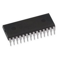
DSPIC30F2010-30I/SPG Microchip Technology, DSPIC30F2010-30I/SPG Datasheet - Page 146

DSPIC30F2010-30I/SPG
Manufacturer Part Number
DSPIC30F2010-30I/SPG
Description
16BIT 30MIPS DSPIC, 30F2010, DIP28
Manufacturer
Microchip Technology
Series
DsPIC30Fr
Datasheet
1.DSPIC30F2010-30ISPG.pdf
(244 pages)
Specifications of DSPIC30F2010-30I/SPG
Core Frequency
30MHz
Embedded Interface Type
I2C, SPI, UART
No. Of I/o's
20
Flash Memory Size
12KB
Supply Voltage Range
2.5V To 5.5V
Operating Temperature Range
-40°C To
Lead Free Status / RoHS Status
Lead free / RoHS Compliant
- Current page: 146 of 244
- Download datasheet (7Mb)
dsPIC30F
20.4
The conversion trigger will terminate acquisition and
start the requested conversions.
The SSRC<2:0> bits select the source of the
conversion trigger.
The SSRC bits provide for up to 5 alternate sources of
conversion trigger.
When SSRC<2:0> = 000, the conversion trigger is
under software control. Clearing the SAMP bit will
cause the conversion trigger.
When SSRC<2:0> = 111 (Auto Start mode), the con-
version trigger is under A/D clock control. The SAMC
bits select the number of A/D clocks between the start
of acquisition and the start of conversion. This provides
the fastest conversion rates on multiple channels.
SAMC must always be at least 1 clock cycle.
Other trigger sources can come from timer modules,
Motor Control PWM module, or external interrupts.
20.5
Clearing the ADON bit during a conversion will abort
the current conversion and stop the sampling sequenc-
ing. The ADCBUF will not be updated with the partially
completed A/D conversion sample. That is, the
ADCBUF will continue to contain the value of the last
completed conversion (or the last value written to the
ADCBUF register).
TABLE 20-1:
DS70082E-page 144
T
T
2 T
4 T
8 T
16 T
32 T
RC
Note 1:
Clock
CY
CY
A/D
CY
CY
CY
A/D Clock Source Select
/2
CY
CY
2:
3:
4:
Programming the Start of
Conversion Trigger
Aborting a Conversion
ADRC
The RC source has a typical T
These values violate the minimum required T
For faster conversion times, the selection of another clock source is recommended.
A/D cannot meet full accuracy with RC clock source and F
0
1
0
0
0
0
0
0
TYPICAL T
ADCS<5:0>
000000
000001
000011
000111
001111
011111
111111
xxxxxx
AD
200-400 ns
1066.56 ns
133.32 ns
533.28 ns
VS. DEVICE OPERATING FREQUENCIES
16.67 ns
33.33 ns
66.66 ns
266.64 ns
30 MHz
AD
time of 300 ns for V
(2)
(2)
(2)
(2)
(3)
(1,4)
(3)
Advance Information
A/D Clock Period (T
200-400 ns
AD
1280 ns
640 ns
25 MHz
20 ns
40 ns
80 ns
time of 154 ns.
160 ns
320 ns
DD
(2)
(2)
(2)
(3)
(3)
(1,4)
> 3.0V.
OSC
AD
If the clearing of the ADON bit coincides with an auto
start, the clearing has a higher priority.
After the A/D conversion is aborted, a 2 T
required before the next sampling may be started by
setting the SAMP bit.
If sequential sampling is specified, the A/D will continue
at the next sample pulse which corresponds with the
next channel converted. If simultaneous sampling is
specified, the A/D will continue with the next
multi-channel group conversion sequence.
20.6
The A/D conversion requires 13 T
A/D conversion clock is software selected using a six
bit counter. There are 64 possible options for T
EQUATION 20-1:
The internal RC oscillator is selected by setting the
ADRC bit.
For correct A/D conversions, the A/D conversion clock
(T
of 154 nsec. Table 20-1 shows the resultant T
derived from the device operating frequencies and the
A/D clock source selected, (for V
AD
Values)
> 20 MHz.
) must be selected to ensure a minimum T
200-400 ns
Device F
12.5 MHz
1.28 µs
2.56 µs
640 ns
40 ns
80 ns
160 ns
320 ns
Selecting the A/D Conversion
Clock
T
AD
(2)
(2)
(3)
(3)
(3)
CY
(1,4)
= T
CY
* (0.5*(ADCS<5:0> +1))
200-400 ns
A/D CONVERSION CLOCK
2004 Microchip Technology Inc.
6.25 MHz
1.28 µs
2.56 µs
5.12 µs
640 ns
80 ns
160 ns
320 ns
(2)
(3)
(3)
(3)
(3)
(1,4)
DD
AD
. The source of the
= 5V).
200-400 ns
16.0 µs
32.0 µs
2.0 µs
4.0 µs
8.0 µs
1 MHz
500 ns
1.0 µs
AD
AD
AD
AD
wait is
(3)
(3)
(3)
(3)
(3)
times
.
time
(1)
Related parts for DSPIC30F2010-30I/SPG
Image
Part Number
Description
Manufacturer
Datasheet
Request
R

Part Number:
Description:
IC DSPIC MCU/DSP 12K 28DIP
Manufacturer:
Microchip Technology
Datasheet:

Part Number:
Description:
IC DSPIC MCU/DSP 12K 28SOIC
Manufacturer:
Microchip Technology
Datasheet:

Part Number:
Description:
IC,DSP,16-BIT,CMOS,SOP,28PIN,PLASTIC
Manufacturer:
Microchip Technology
Datasheet:

Part Number:
Description:
IC DSPIC MCU/DSP 12K 28SOIC
Manufacturer:
Microchip Technology
Datasheet:

Part Number:
Description:
IC DSPIC MCU/DSP 12K 28QFN
Manufacturer:
Microchip Technology
Datasheet:

Part Number:
Description:
IC DSPIC MCU/DSP 12K 28QFN
Manufacturer:
Microchip Technology
Datasheet:

Part Number:
Description:
IC DSPIC MCU/DSP 12K 28DIP
Manufacturer:
Microchip Technology
Datasheet:

Part Number:
Description:
IC DSPIC MCU/DSP 12K 28SOIC
Manufacturer:
Microchip Technology
Datasheet:

Part Number:
Description:
IC DSPIC MCU/DSP 12K 28DIP
Manufacturer:
Microchip Technology
Datasheet:

Part Number:
Description:
IC DSPIC MCU/DSP 12K 28SOIC
Manufacturer:
Microchip Technology

Part Number:
Description:
IC DSPIC MCU/DSP 12K 28QFN
Manufacturer:
Microchip Technology

Part Number:
Description:
IC DSPIC MCU/DSP 12K 28DIP
Manufacturer:
Microchip Technology

Part Number:
Description:
IC,DSP,16-BIT,CMOS,LLCC,28PIN,PLASTIC
Manufacturer:
Microchip Technology
Datasheet:

Part Number:
Description:
Digital Signal Processors & Controllers - DSP, DSC
Manufacturer:
Microchip Technology

Part Number:
Description:
Digital Signal Processors & Controllers - DSP, DSC 16 Bit MCU/DSP 28LD 20M 12KB FL
Manufacturer:
Microchip Technology


