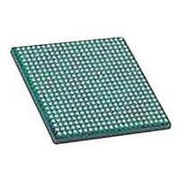
LFXP2-40E-5FN672C LATTICE SEMICONDUCTOR, LFXP2-40E-5FN672C Datasheet - Page 19

LFXP2-40E-5FN672C
Manufacturer Part Number
LFXP2-40E-5FN672C
Description
IC, LATTICEXP2 FPGA, 435MHZ, FPBGA-672
Manufacturer
LATTICE SEMICONDUCTOR
Series
LatticeXP2r
Datasheet
1.LFXP2-5E-5TN144C.pdf
(93 pages)
Specifications of LFXP2-40E-5FN672C
No. Of Logic Blocks
40000
No. Of Macrocells
20000
Family Type
LatticeXP2
No. Of Speed Grades
5
No. Of I/o's
540
Clock Management
PLL
Total Ram Bits
885Kbit
Lead Free Status / RoHS Status
Lead free / RoHS Compliant
- Current page: 19 of 93
- Download datasheet (2Mb)
Lattice Semiconductor
Table 2-5. sysMEM Block Configurations
Bus Size Matching
All of the multi-port memory modes support different widths on each of the ports. The RAM bits are mapped LSB
word 0 to MSB word 0, LSB word 1 to MSB word 1, and so on. Although the word size and number of words for
each port varies, this mapping scheme applies to each port.
FlashBAK EBR Content Storage
All the EBR memory in the LatticeXP2 is shadowed by Flash memory. Optionally, initialization values for the mem-
ory blocks can be defined using the Lattice ispLEVER tools. The initialization values are loaded into the Flash
memory during device programming and into the SRAM at power up or whenever the device is reconfigured. This
feature is ideal for the storage of a variety of information such as look-up tables and microprocessor code. It is also
possible to write the current contents of the EBR memory back to Flash memory. This capability is useful for the
storage of data such as error codes and calibration information. For additional information on the FlashBAK capa-
bility see TN1141, LatticeXP2 sysCONFIG Usage Guide.
Figure 2-16. FlashBAK Technology
Memory Cascading
Larger and deeper blocks of RAMs can be created using EBR sysMEM Blocks. Typically, the Lattice design tools
cascade memory transparently, based on specific design inputs.
Single, Dual and Pseudo-Dual Port Modes
In all the sysMEM RAM modes the input data and address for the ports are registered at the input of the memory
array. The output data of the memory is optionally registered at the output.
FPGA Logic
Make Infinite Reads and
Writes to EBR
Single Port
True Dual Port
Pseudo Dual Port
Memory Mode
EBR
2-16
Flash
Configurations
16,384 x 1
1,024 x 18
16,384 x 1
1,024 x 18
16,384 x 1
1,024 x 18
8,192 x 2
4,096 x 4
2,048 x 9
8,192 x 2
4,096 x 4
2,048 x 9
8,192 x 2
4,096 x 4
2,048 x 9
512 x 36
512 x 36
EBR During Configuration /
Write From EBR to Flash
Write to Flash During
Write From Flash to
on User Command
Programming
LatticeXP2 Family Data Sheet
JTAG / SPI Port
Architecture
Related parts for LFXP2-40E-5FN672C
Image
Part Number
Description
Manufacturer
Datasheet
Request
R

Part Number:
Description:
IC, LATTICEXP2 FPGA, 435MHZ, FPBGA-484
Manufacturer:
LATTICE SEMICONDUCTOR
Datasheet:
Part Number:
Description:
ISPLSI2032-80LT44Lattice Semiconductor [In-System Programmable High Density PLD]
Manufacturer:
Lattice Semiconductor Corp.
Datasheet:
Part Number:
Description:
IC PROGRAMMED LATTICE GAL 16V8
Manufacturer:
Lattice Semiconductor Corp.
Datasheet:
Part Number:
Description:
357-036-542-201 CARDEDGE 36POS DL .156 BLK LOPRO
Manufacturer:
Lattice Semiconductor Corp.
Datasheet:
Part Number:
Description:
357-036-542-201 CARDEDGE 36POS DL .156 BLK LOPRO
Manufacturer:
Lattice Semiconductor Corp.
Datasheet:
Part Number:
Description:
357-036-542-201 CARDEDGE 36POS DL .156 BLK LOPRO
Manufacturer:
Lattice Semiconductor Corp.
Datasheet:
Part Number:
Description:
357-036-542-201 CARDEDGE 36POS DL .156 BLK LOPRO
Manufacturer:
Lattice Semiconductor Corp.
Datasheet:
Part Number:
Description:
357-036-542-201 CARDEDGE 36POS DL .156 BLK LOPRO
Manufacturer:
Lattice Semiconductor Corp.
Datasheet:
Part Number:
Description:
357-036-542-201 CARDEDGE 36POS DL .156 BLK LOPRO
Manufacturer:
Lattice Semiconductor Corp.
Datasheet:
Part Number:
Description:
357-036-542-201 CARDEDGE 36POS DL .156 BLK LOPRO
Manufacturer:
Lattice Semiconductor Corp.
Datasheet:
Part Number:
Description:
357-036-542-201 CARDEDGE 36POS DL .156 BLK LOPRO
Manufacturer:
Lattice Semiconductor Corp.
Datasheet:
Part Number:
Description:
357-036-542-201 CARDEDGE 36POS DL .156 BLK LOPRO
Manufacturer:
Lattice Semiconductor Corp.
Datasheet:
Part Number:
Description:
357-036-542-201 CARDEDGE 36POS DL .156 BLK LOPRO
Manufacturer:
Lattice Semiconductor Corp.
Datasheet:
Part Number:
Description:
In-system programmable 3.3V generic digital switch
Manufacturer:
Lattice Semiconductor Corp.
Datasheet:
Part Number:
Description:
High performance E2CMOS PLD generic array logic, 15ns, quarter power
Manufacturer:
Lattice Semiconductor Corp.
Datasheet:


