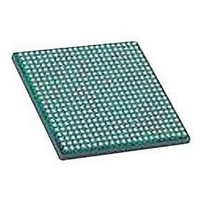
LFXP2-40E-5FN672C LATTICE SEMICONDUCTOR, LFXP2-40E-5FN672C Datasheet - Page 65

LFXP2-40E-5FN672C
Manufacturer Part Number
LFXP2-40E-5FN672C
Description
IC, LATTICEXP2 FPGA, 435MHZ, FPBGA-672
Manufacturer
LATTICE SEMICONDUCTOR
Series
LatticeXP2r
Datasheet
1.LFXP2-5E-5TN144C.pdf
(93 pages)
Specifications of LFXP2-40E-5FN672C
No. Of Logic Blocks
40000
No. Of Macrocells
20000
Family Type
LatticeXP2
No. Of Speed Grades
5
No. Of I/o's
540
Clock Management
PLL
Total Ram Bits
885Kbit
Lead Free Status / RoHS Status
Lead free / RoHS Compliant
- Current page: 65 of 93
- Download datasheet (2Mb)
Lattice Semiconductor
LatticeXP2 Internal Switching Characteristics
t
t
t
t
t
t
t
t
1. Internal parameters are characterized, but not tested on every device.
2. RST resets VCO and all counters in PLL.
3. These parameters include the Adder Subtractor block in the path.
Timing v. A 0.10
HP_DSP
SUO_DSP
HO_DSP
COI_DSP
COP_DSP
COO_DSP
SUADSUB
HADSUB
Parameter
3
3
3
Pipeline Register Hold Time
Output Register Setup Time
Output Register Hold Time
Input Register Clock to Output
Time
Pipeline Register Clock to Output
Time
Output Register Clock to Output
Time
AdSub Input Register Setup Time
AdSub Input Register Hold Time
Description
Over Recommended Operating Conditions
-0.787
-1.439
-0.270
4.896
0.306
Min.
—
—
—
-7
3-21
4.513
2.153
0.569
Max.
—
—
—
—
—
-0.890
-1.604
-0.298
5.413
0.338
Min.
1
—
—
—
(Continued)
DC and Switching Characteristics
-6
LatticeXP2 Family Data Sheet
4.947
2.272
0.600
Max.
—
—
—
—
—
-0.994
-1.770
-0.327
5.931
0.371
Min.
—
—
—
-5
5.382
2.391
0.631
Max.
—
—
—
—
—
Units
ns
ns
ns
ns
ns
ns
ns
ns
Related parts for LFXP2-40E-5FN672C
Image
Part Number
Description
Manufacturer
Datasheet
Request
R

Part Number:
Description:
IC, LATTICEXP2 FPGA, 435MHZ, FPBGA-484
Manufacturer:
LATTICE SEMICONDUCTOR
Datasheet:
Part Number:
Description:
ISPLSI2032-80LT44Lattice Semiconductor [In-System Programmable High Density PLD]
Manufacturer:
Lattice Semiconductor Corp.
Datasheet:
Part Number:
Description:
IC PROGRAMMED LATTICE GAL 16V8
Manufacturer:
Lattice Semiconductor Corp.
Datasheet:
Part Number:
Description:
357-036-542-201 CARDEDGE 36POS DL .156 BLK LOPRO
Manufacturer:
Lattice Semiconductor Corp.
Datasheet:
Part Number:
Description:
357-036-542-201 CARDEDGE 36POS DL .156 BLK LOPRO
Manufacturer:
Lattice Semiconductor Corp.
Datasheet:
Part Number:
Description:
357-036-542-201 CARDEDGE 36POS DL .156 BLK LOPRO
Manufacturer:
Lattice Semiconductor Corp.
Datasheet:
Part Number:
Description:
357-036-542-201 CARDEDGE 36POS DL .156 BLK LOPRO
Manufacturer:
Lattice Semiconductor Corp.
Datasheet:
Part Number:
Description:
357-036-542-201 CARDEDGE 36POS DL .156 BLK LOPRO
Manufacturer:
Lattice Semiconductor Corp.
Datasheet:
Part Number:
Description:
357-036-542-201 CARDEDGE 36POS DL .156 BLK LOPRO
Manufacturer:
Lattice Semiconductor Corp.
Datasheet:
Part Number:
Description:
357-036-542-201 CARDEDGE 36POS DL .156 BLK LOPRO
Manufacturer:
Lattice Semiconductor Corp.
Datasheet:
Part Number:
Description:
357-036-542-201 CARDEDGE 36POS DL .156 BLK LOPRO
Manufacturer:
Lattice Semiconductor Corp.
Datasheet:
Part Number:
Description:
357-036-542-201 CARDEDGE 36POS DL .156 BLK LOPRO
Manufacturer:
Lattice Semiconductor Corp.
Datasheet:
Part Number:
Description:
357-036-542-201 CARDEDGE 36POS DL .156 BLK LOPRO
Manufacturer:
Lattice Semiconductor Corp.
Datasheet:
Part Number:
Description:
In-system programmable 3.3V generic digital switch
Manufacturer:
Lattice Semiconductor Corp.
Datasheet:
Part Number:
Description:
High performance E2CMOS PLD generic array logic, 15ns, quarter power
Manufacturer:
Lattice Semiconductor Corp.
Datasheet:


