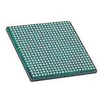
LFXP2-40E-5FN672C LATTICE SEMICONDUCTOR, LFXP2-40E-5FN672C Datasheet - Page 53

LFXP2-40E-5FN672C
Manufacturer Part Number
LFXP2-40E-5FN672C
Description
IC, LATTICEXP2 FPGA, 435MHZ, FPBGA-672
Manufacturer
LATTICE SEMICONDUCTOR
Series
LatticeXP2r
Datasheet
1.LFXP2-5E-5TN144C.pdf
(93 pages)
Specifications of LFXP2-40E-5FN672C
No. Of Logic Blocks
40000
No. Of Macrocells
20000
Family Type
LatticeXP2
No. Of Speed Grades
5
No. Of I/o's
540
Clock Management
PLL
Total Ram Bits
885Kbit
Lead Free Status / RoHS Status
Lead free / RoHS Compliant
- Current page: 53 of 93
- Download datasheet (2Mb)
Lattice Semiconductor
Table 3-1. LVDS25E DC Conditions
LVCMOS33D
All I/O banks support emulated differential I/O using the LVCMOS33D I/O type. This option, along with the external
resistor network, provides the system designer the flexibility to place differential outputs on an I/O bank with 3.3V
VCCIO. The default drive current for LVCMOS33D output is 12mA with the option to change the device strength to
4mA, 8mA, 16mA or 20mA. Follow the LVCMOS33 specifications for the DC characteristics of the LVCMOS33D.
V
Z
R
R
R
V
V
V
V
Z
I
DC
Parameter
OUT
OH
OL
OD
BACK
CCIO
T
CM
S
P
Output Driver Supply (+/-5%)
Driver Impedance
Driver Series Resistor (+/-1%)
Driver Parallel Resistor (+/-1%)
Receiver Termination (+/-1%)
Output High Voltage (after R
Output Low Voltage (after R
Output Differential Voltage (After R
Output Common Mode Voltage
Back Impedance
DC Output Current
Description
1
1
3-9
)
)
1
)
Typical
DC and Switching Characteristics
100.5
2.50
1.43
1.07
0.35
1.25
6.03
158
140
100
20
LatticeXP2 Family Data Sheet
Units
mA
Ω
Ω
Ω
Ω
Ω
V
V
V
V
V
Related parts for LFXP2-40E-5FN672C
Image
Part Number
Description
Manufacturer
Datasheet
Request
R

Part Number:
Description:
IC, LATTICEXP2 FPGA, 435MHZ, FPBGA-484
Manufacturer:
LATTICE SEMICONDUCTOR
Datasheet:
Part Number:
Description:
ISPLSI2032-80LT44Lattice Semiconductor [In-System Programmable High Density PLD]
Manufacturer:
Lattice Semiconductor Corp.
Datasheet:
Part Number:
Description:
IC PROGRAMMED LATTICE GAL 16V8
Manufacturer:
Lattice Semiconductor Corp.
Datasheet:
Part Number:
Description:
357-036-542-201 CARDEDGE 36POS DL .156 BLK LOPRO
Manufacturer:
Lattice Semiconductor Corp.
Datasheet:
Part Number:
Description:
357-036-542-201 CARDEDGE 36POS DL .156 BLK LOPRO
Manufacturer:
Lattice Semiconductor Corp.
Datasheet:
Part Number:
Description:
357-036-542-201 CARDEDGE 36POS DL .156 BLK LOPRO
Manufacturer:
Lattice Semiconductor Corp.
Datasheet:
Part Number:
Description:
357-036-542-201 CARDEDGE 36POS DL .156 BLK LOPRO
Manufacturer:
Lattice Semiconductor Corp.
Datasheet:
Part Number:
Description:
357-036-542-201 CARDEDGE 36POS DL .156 BLK LOPRO
Manufacturer:
Lattice Semiconductor Corp.
Datasheet:
Part Number:
Description:
357-036-542-201 CARDEDGE 36POS DL .156 BLK LOPRO
Manufacturer:
Lattice Semiconductor Corp.
Datasheet:
Part Number:
Description:
357-036-542-201 CARDEDGE 36POS DL .156 BLK LOPRO
Manufacturer:
Lattice Semiconductor Corp.
Datasheet:
Part Number:
Description:
357-036-542-201 CARDEDGE 36POS DL .156 BLK LOPRO
Manufacturer:
Lattice Semiconductor Corp.
Datasheet:
Part Number:
Description:
357-036-542-201 CARDEDGE 36POS DL .156 BLK LOPRO
Manufacturer:
Lattice Semiconductor Corp.
Datasheet:
Part Number:
Description:
357-036-542-201 CARDEDGE 36POS DL .156 BLK LOPRO
Manufacturer:
Lattice Semiconductor Corp.
Datasheet:
Part Number:
Description:
In-system programmable 3.3V generic digital switch
Manufacturer:
Lattice Semiconductor Corp.
Datasheet:
Part Number:
Description:
High performance E2CMOS PLD generic array logic, 15ns, quarter power
Manufacturer:
Lattice Semiconductor Corp.
Datasheet:


