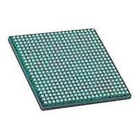
LFXP2-17E-5FN484C8W LATTICE SEMICONDUCTOR, LFXP2-17E-5FN484C8W Datasheet - Page 13

LFXP2-17E-5FN484C8W
Manufacturer Part Number
LFXP2-17E-5FN484C8W
Description
IC, LATTICEXP2 FPGA, 435MHZ, FPBGA-484
Manufacturer
LATTICE SEMICONDUCTOR
Series
LatticeXP2r
Datasheet
1.LFXP2-5E-5TN144C.pdf
(93 pages)
Specifications of LFXP2-17E-5FN484C8W
No. Of Logic Blocks
17000
No. Of Macrocells
8500
Family Type
LatticeXP2
No. Of Speed Grades
5
No. Of I/o's
358
Clock Management
PLL
Total Ram Bits
276Kbit
Lead Free Status / RoHS Status
Lead free / RoHS Compliant
Available stocks
Company
Part Number
Manufacturer
Quantity
Price
Company:
Part Number:
LFXP2-17E-5FN484C8W
Manufacturer:
NPC
Quantity:
319
Part Number:
LFXP2-17E-5FN484C8W
Manufacturer:
LATIICE
Quantity:
20 000
Lattice Semiconductor
Secondary Clock/Control Sources
LatticeXP2 devices derive secondary clocks (SC0 through SC7) from eight dedicated clock input pads and the rest
from routing. Figure 2-7 shows the secondary clock sources.
Figure 2-7. Secondary Clock Sources
Clock Input
Clock Input
From Routing
From Routing
From Routing
From Routing
Routing
Routing
From
From
Routing
Routing
From
From
Secondary Clock Sources
Clock
Clock
Input
Input
2-10
Clock
Clock
Input
Input
Routing
Routing
From
From
LatticeXP2 Family Data Sheet
Routing
Routing
From
From
From Routing
From Routing
From Routing
From Routing
Clock Input
Clock Input
Architecture


