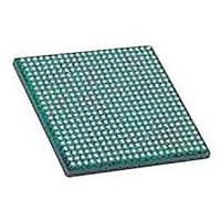
LFXP2-17E-5FN484C8W LATTICE SEMICONDUCTOR, LFXP2-17E-5FN484C8W Datasheet - Page 47

LFXP2-17E-5FN484C8W
Manufacturer Part Number
LFXP2-17E-5FN484C8W
Description
IC, LATTICEXP2 FPGA, 435MHZ, FPBGA-484
Manufacturer
LATTICE SEMICONDUCTOR
Series
LatticeXP2r
Datasheet
1.LFXP2-5E-5TN144C.pdf
(93 pages)
Specifications of LFXP2-17E-5FN484C8W
No. Of Logic Blocks
17000
No. Of Macrocells
8500
Family Type
LatticeXP2
No. Of Speed Grades
5
No. Of I/o's
358
Clock Management
PLL
Total Ram Bits
276Kbit
Lead Free Status / RoHS Status
Lead free / RoHS Compliant
Available stocks
Company
Part Number
Manufacturer
Quantity
Price
Company:
Part Number:
LFXP2-17E-5FN484C8W
Manufacturer:
NPC
Quantity:
319
Part Number:
LFXP2-17E-5FN484C8W
Manufacturer:
LATIICE
Quantity:
20 000
Lattice Semiconductor
Supply Current (Standby)
I
I
I
I
I
1. For further information on supply current, please see TN1139, Power Estimation and Management for LatticeXP2 Devices.
2. Assumes all outputs are tristated, all inputs are configured as LVCMOS and held at the V
3. Frequency 0MHz.
4. Pattern represents a “blank” configuration data file.
5. T
6. In fpBGA and ftBGA packages the PLLs are connected to and powered from the auxiliary power supply. For these packages,
CC
CCAUX
CCPLL
CCIO
CCJ
the actual auxiliary supply current is the sum of I
powered independent of the auxiliary power supply.
J
= 25
Symbol
o
C, power supplies at nominal voltage.
Core Power Supply Current
Auxiliary Power Supply Current
PLL Power Supply Current (per PLL)
Bank Power Supply Current (per bank)
V
CCJ
Power Supply Current
Over Recommended Operating Conditions
1, 2, 3, 4
Parameter
CCAUX
6
and I
3-3
CCPLL.
For csBGA, PQFP and TQFP packages the PLLs are
XP2-5
XP2-8
XP2-17
XP2-30
XP2-40
XP2-5
XP2-8
XP2-17
XP2-30
XP2-40
Device
DC and Switching Characteristics
LatticeXP2 Family Data Sheet
CCIO
or GND.
Typical
0.25
0.1
14
18
24
35
45
15
15
15
16
16
2
5
Units
mA
mA
mA
mA
mA
mA
mA
mA
mA
mA
mA
mA
mA


