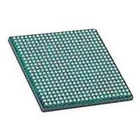
LFXP2-17E-5FN484C8W LATTICE SEMICONDUCTOR, LFXP2-17E-5FN484C8W Datasheet - Page 80

LFXP2-17E-5FN484C8W
Manufacturer Part Number
LFXP2-17E-5FN484C8W
Description
IC, LATTICEXP2 FPGA, 435MHZ, FPBGA-484
Manufacturer
LATTICE SEMICONDUCTOR
Series
LatticeXP2r
Datasheet
1.LFXP2-5E-5TN144C.pdf
(93 pages)
Specifications of LFXP2-17E-5FN484C8W
No. Of Logic Blocks
17000
No. Of Macrocells
8500
Family Type
LatticeXP2
No. Of Speed Grades
5
No. Of I/o's
358
Clock Management
PLL
Total Ram Bits
276Kbit
Lead Free Status / RoHS Status
Lead free / RoHS Compliant
Available stocks
Company
Part Number
Manufacturer
Quantity
Price
Company:
Part Number:
LFXP2-17E-5FN484C8W
Manufacturer:
NPC
Quantity:
319
Part Number:
LFXP2-17E-5FN484C8W
Manufacturer:
LATIICE
Quantity:
20 000
Lattice Semiconductor
PICs and DDR Data (DQ) Pins Associated with the DDR Strobe (DQS) Pin
For Left and Right Edges of the Device
P[Edge] [n-4]
P[Edge] [n-3]
P[Edge] [n-2]
P[Edge] [n-1]
P[Edge] [n]
P[Edge] [n+1]
P[Edge] [n+2]
P[Edge] [n+3]
For Top and Bottom Edges of the Device
P[Edge] [n-4]
P[Edge] [n-3]
P[Edge] [n-2]
P[Edge] [n-1]
P[Edge] [n]
P[Edge] [n+1]
P[Edge] [n+2]
P[Edge] [n+3]
P[Edge] [n+4]
Notes:
1. “n” is a row PIC number.
2. The DDR interface is designed for memories that support one DQS strobe up to 16 bits
PICs Associated with
of data for the left and right edges and up to 18 bits of data for the top and bottom
edges. In some packages, all the potential DDR data (DQ) pins may not be available.
PIC numbering definitions are provided in the “Signal Names” column of the Signal
Descriptions table.
DQS Strobe
PIO Within PIC
4-3
A
B
A
B
A
B
A
B
A
B
A
B
A
B
A
B
A
B
A
B
A
B
A
B
A
B
A
B
A
B
A
B
A
B
DDR Strobe (DQS) and
Data (DQ) Pins
[Edge]DQSn
[Edge]DQSn
LatticeXP2 Family Data Sheet
DQ
DQ
DQ
DQ
DQ
DQ
DQ
DQ
DQ
DQ
DQ
DQ
DQ
DQ
DQ
DQ
DQ
DQ
DQ
DQ
DQ
DQ
DQ
DQ
DQ
DQ
DQ
DQ
DQ
DQ
DQ
DQ
Pinout Information


