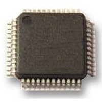
LPC2106FBD48/01 NXP Semiconductors, LPC2106FBD48/01 Datasheet - Page 13

LPC2106FBD48/01
Manufacturer Part Number
LPC2106FBD48/01
Description
IC, MCU, 32BIT, 128K FLASH, 48LQFP
Manufacturer
NXP Semiconductors
Datasheet
1.LPC2105FBD48.pdf
(41 pages)
Specifications of LPC2106FBD48/01
Controller Family/series
ARM7
No. Of I/o's
32
Ram Memory Size
64KB
Cpu Speed
60MHz
No. Of Timers
3
No. Of Pwm
RoHS Compliant
Core Size
32bit
Program Memory Size
128KB
Oscillator Type
Internal, External
Available stocks
Company
Part Number
Manufacturer
Quantity
Price
Company:
Part Number:
LPC2106FBD48/01
Manufacturer:
NXP
Quantity:
670
Company:
Part Number:
LPC2106FBD48/01
Manufacturer:
NXP
Quantity:
7 750
Company:
Part Number:
LPC2106FBD48/01,15
Manufacturer:
NXP
Quantity:
250
Company:
Part Number:
LPC2106FBD48/01,15
Manufacturer:
NXP Semiconductors
Quantity:
10 000
NXP Semiconductors
LPC2104_2105_2106_7
Product data sheet
6.6 Pin connect block
6.7 Pin function select register 0 (PINSEL0 - 0xE002 C000)
Table 4.
[1]
The pin connect block allows selected pins of the microcontroller to have more than one
function. Configuration registers control the multiplexers to allow connection between the
pin and the on chip peripherals. Peripherals should be connected to the appropriate pins
prior to being activated, and prior to any related interrupt(s) being enabled. Activity of any
enabled peripheral function that is not mapped to a related pin should be considered
undefined.
The Pin Control Module contains two registers as shown in
Table 5.
The PINSEL0 register controls the functions of the pins as per the settings listed in
Table
function is selected for a pin. For other functions, direction is controlled automatically.
Settings other than those shown in
Block
UART 1
PWM0
I
SPI and SSP
-
PLL
RTC
System Control
System Control
System Control
Address
0xE002 C000
0xE002 C004
2
C-bus
Available on LPC2104/2105/2106/01 only.
6. The direction control bit in the IODIR register is effective only when the GPIO
Interrupt sources
Pin control module registers
[1]
Flag(s)
Rx Line Status (RLS)
Transmit Holding Register empty (THRE)
Rx Data Available (RDA)
Character Time-out Indicator (CTI)
Modem Status Interrupt (MSI)
Auto-Baud Time-Out (ABTO)
End of Auto-Baud (ABEO)
Match 0 to 6 (MR0, MR1, MR2, MR3, MR4, MR5, MR6)
SI (state change)
SPIF, MODF (SPI)
TXRIS, RXRIS, RTRIS, RORRIS (SSP)
reserved
PLL Lock (PLOCK)
RTCCIF (Counter Increment), RTCALF (Alarm)
External Interrupt 0 (EINT0)
External Interrupt 1 (EINT1)
External Interrupt 2 (EINT2)
Name
PINSEL0
PINSEL1
Rev. 07 — 20 June 2008
…continued
Table 6
Description
Pin function select register 0
Pin function select register 1
[1]
[1]
are reserved, and should not be used
LPC2104/2105/2106
Single-chip 32-bit microcontrollers
[1]
Table
5.
© NXP B.V. 2008. All rights reserved.
Access
Read/Write
Read/Write
VIC channel #
7
8
9
10
11
12
13
14
15
16
13 of 41


