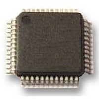
MB96F313ASBPMC-GSE2 Fujitsu, MB96F313ASBPMC-GSE2 Datasheet - Page 44

MB96F313ASBPMC-GSE2
Manufacturer Part Number
MB96F313ASBPMC-GSE2
Description
MCU, 16BIT, 16FX, 96K FLASH, 48LQFP
Manufacturer
Fujitsu
Datasheet
1.MB96F313ASBPMC-GSE2.pdf
(84 pages)
Specifications of MB96F313ASBPMC-GSE2
No. Of I/o's
36
Ram Memory Size
8KB
Cpu Speed
56MHz
No. Of Timers
3
No. Of Pwm Channels
14
Digital Ic Case
RoHS Compliant
Core Size
16bit
Program Memory Size
96KB
Oscillator Type
Internal, External
Controller Family/series
MB96310
MB96310 Series
4. Unused sub clock signal
5. Notes on PLL clock mode operation
6. Power supply pins (V
7. Crystal oscillator and ceramic resonator circuit
8. Turn on sequence of power supply to A/D converter and analog inputs
9. Pin handling when not using the A/D converter
10. Notes on Power-on
44
2. Opposite phase external clock
• When using an opposite phase external clock, X1 (X1A) must be supplied with a clock signal which has the
If the pins X0A and X1A are not connected to an oscillator, a pull-down resistor must be connected on the X0A
pin and the X1A pin must be left open.
If the PLL clock mode is selected and no external oscillator is operating or no external clock is supplied, the
microcontroller attempts to work with the free oscillating PLL. Performance of this operation, however, cannot
be guaranteed.
It is required that all V
than one V
range.
V
As a measure against power supply noise, it is required to connect a bypass capacitor of about 0.1 μF between
V
Noise at X0, X1 pins or X0A, X1A pins might cause abnormal operation. It is required to provide bypass capacitors
with shortest possible distance to X0, X1 pins and X0A, X1A pins, crystal oscillator (or ceramic resonator) and
ground lines, and, to the utmost effort, that the lines of oscillation circuit do not cross the lines of other circuits.
It is highly recommended to provide a printed circuit board art work surrounding X0, X1 pins and X0A, X1A pins
with a ground area for stabilizing the operation.
It is highly recommended to evaluate the quartz/MCU or resonator/MCU system at the quartz or resonator
manufacturer, especially when using low-Q resonators at higher frequencies.
It is required to turn the A/D converter power supply (AV
turning the digital power supply (V
It is also required to turn the digital power off after turning the A/D converter supply and analog inputs off. In this
case, the voltage must not exceed AVRH or AV
on or off is acceptable).
It is required to connect the unused pins of the A/D converter as AV
To prevent malfunction of the internal voltage regulator, supply voltage profile while turning the power supply on
should be slower than 50μs from 0.2 V to 2.7 V.
CC
CC
opposite phase to the X0 (X0A) pins.
and V
and V
SS
SS
CC
must be connected to the device from the power supply with lowest possible impedance.
as close as possible to V
or V
SS
level, the device may operate incorrectly or be damaged even within the guaranteed operating
CC
-level as well as all V
CC
/
V
SS
)
CC
) on.
CC
and V
SS
-level power supply pins are at the same potential. If there is more
SS
CC
pins.
(turning the analog and digital power supplies simultaneously
CC
, AVRH, AVRL) and analog inputs (ANn) on after
CC
X0
X1
= V
CC
,
AV
SS
= AVRH = AVRL = V
DS07-13808-2E
SS
.


