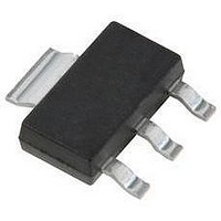
S-812C33AUA-C2N-T2G Seiko Instruments, S-812C33AUA-C2N-T2G Datasheet - Page 16

S-812C33AUA-C2N-T2G
Manufacturer Part Number
S-812C33AUA-C2N-T2G
Description
IC, LINEAR VOLT REGULATOR, 3.3V, SOT89-3
Manufacturer
Seiko Instruments
Datasheet
1.S-812C33AUA-C2N-T2G.pdf
(52 pages)
Specifications of S-812C33AUA-C2N-T2G
Primary Input Voltage
5.3V
Output Voltage Fixed
3.3V
Dropout Voltage Vdo
120mV
No. Of Outputs
1
No. Of Pins
3
Output Current
50mA
Operating Temperature Range
-40°C To +85°C
Lead Free Status / RoHS Status
Lead free / RoHS Compliant
16
HIGH OPERATING VOLTAGE CMOS VOLTAGE REGULATOR
S-812C Series
Operation
1. Basic Operation
2. Output Transistor
Figure 16 shows the block diagram of the S-812C Series.
The error amplifier compares the reference voltage (V
divided by feedback resistors R
output voltage which is not influenced by the input voltage and temperature change, to the output
transistor.
In the S-812C Series, a low on-resistance P-channel MOS FET is used as the output transistor.
Be sure that V
to inverse current which flows, because of a parasitic diode between the VIN and VOUT pin.
Current supply
OUT
VSS
VIN
*1. Parasitic diode
does not exceed V
V
Reference
ref
voltage
circuit
s
and R
Error amplifier
IN
Seiko Instruments Inc.
+ 0.3 V to prevent the voltage regulator from being damaged due
f
. It supplies the gate voltage necessary to maintain the constant
+
−
Figure 16
ref
) with V
fb
R
R
, which is the output voltage resistance-
f
S
*1
VOUT
Rev.4.1
_00


