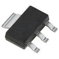
S-812C33AUA-C2N-T2G Seiko Instruments, S-812C33AUA-C2N-T2G Datasheet - Page 19

S-812C33AUA-C2N-T2G
Manufacturer Part Number
S-812C33AUA-C2N-T2G
Description
IC, LINEAR VOLT REGULATOR, 3.3V, SOT89-3
Manufacturer
Seiko Instruments
Datasheet
1.S-812C33AUA-C2N-T2G.pdf
(52 pages)
Specifications of S-812C33AUA-C2N-T2G
Primary Input Voltage
5.3V
Output Voltage Fixed
3.3V
Dropout Voltage Vdo
120mV
No. Of Outputs
1
No. Of Pins
3
Output Current
50mA
Operating Temperature Range
-40°C To +85°C
Lead Free Status / RoHS Status
Lead free / RoHS Compliant
Rev.4.1
2. Constant Current Circuit
3. Output Voltage Adjustment Circuit
(Only for S-812CxxA Series (No short-circuit protection, power-off function))
This circuit can be used as a constant current circuit if making the composition seen in Figure 19 and 20.
Constant current I
Note that by using a circuit in Figure 19, it is impossible to set the better driving ability to the constant
amperage (I
To gain the driving ability which exceeds the S-812C Series, there’s a way to combine a constant
current circuit and a current boosting circuit, as seen in Figure 20.
The maximum input voltage for a constant current circuit is 16 V + the voltage for device (V
It is not recommended to add a capacitor between the VIN (power supply) and VSS pin or the VOUT
(output) and VSS pin because the rush current flows at power-on.
Set the value of resistors R1 and R2 so that the S-812C Series is not affected by current consumption
I
Capacitor C
value according to the actual evaluation.
It is not recommended to add a capacitor between the VIN (power supply) and VSS pin or the VOUT
(output) and VSS pin because it causes output fluctuation and output oscillation due to power-on.
By using the composition seen in Figure 21, users are able to increase the output voltage. The value of
output voltage V
V
(V
I
(V
SS
O
OUT1
= (V
.
OUT(E)
OUT(E)
_00
= V
OUT(E)
= effective output voltage)
= effective output voltage)
OUT(E)
1
O
÷ R
) than the S-812C Series basically has.
reduces output fluctuation due to power-on, power fluctuation and load fluctuation. Set the
× (R
L
) + I
OUT1
O
is calculated from the following equation:
1
SS
is calculated from the following equation:
+ R
2
HIGH OPERATING VOLTAGE CMOS VOLTAGE REGULATOR
) ÷ R
GND
V
GND
IN
V
V
GND
IN
Figure 20 Constant Current Boost Circuit
IN
1
+ R
VIN
Figure 19 Constant Current Circuit
C
2
IN
VSS
× I
Seiko Instruments Inc.
S-812C
Series
C
ON/OFF
SS
C
C
R
IN
VIN
IN
1
1
Tr1
VSS
S-812C
Series
VIN
Figure 21
VSS
S-812C
Series
VOUT
ON/OFF
VOUT
VOUT
V
V
R
R
O
O
1
2
R
R
L
L
I
I
O
O
V
V
OUT
OUT
V
C
Device
OUT1
Device
L
S-812C Series
O
).
19


