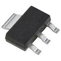
S-812C33AUA-C2N-T2G Seiko Instruments, S-812C33AUA-C2N-T2G Datasheet - Page 18

S-812C33AUA-C2N-T2G
Manufacturer Part Number
S-812C33AUA-C2N-T2G
Description
IC, LINEAR VOLT REGULATOR, 3.3V, SOT89-3
Manufacturer
Seiko Instruments
Datasheet
1.S-812C33AUA-C2N-T2G.pdf
(52 pages)
Specifications of S-812C33AUA-C2N-T2G
Primary Input Voltage
5.3V
Output Voltage Fixed
3.3V
Dropout Voltage Vdo
120mV
No. Of Outputs
1
No. Of Pins
3
Output Current
50mA
Operating Temperature Range
-40°C To +85°C
Lead Free Status / RoHS Status
Lead free / RoHS Compliant
18
HIGH OPERATING VOLTAGE CMOS VOLTAGE REGULATOR
S-812C Series
Selection of External Components
Application Circuit
1. Output Capacitor (C
1. Output Current Boost Circuit
The S-812C Series has an internal phase compensation circuit which stabilizes the operation regardless
of the change of output load. Therefore it is possible for users to have a stable operation without an
output capacitor (C
characteristics of transient response, vary depending on the output capacitor. In selecting the value of
output capacitor, refer to the data on C
characteristics”.
Set ESR 10 Ω or less when using a tantalum capacitor or an aluminum electrolytic capacitor. Pay
attention at low temperature, that aluminum electrolytic capacitor especially may oscillate because ESR
increases. Evaluate sufficiently including the temperature characteristics in use.
As shown in Figure 18, the output current can be boosted by externally attaching a PNP transistor.
Between the input voltage V
base-emitter voltage VBE which fully switches the PNP transistor on, S-812C Series controls the base
current in a PNP transistor so that the output voltage V
the S-812C Series.
Since the output current boosting circuit in Figure 18 does not have the good characteristics of transient
response, under the usage condition, confirm if output fluctuation due to power-on, and fluctuations of
power supply and load affect on the operation or not before use.
Note that the short-circuit protection circuit in the S-812C Series does not work as short-circuit protection
for this boost circuit.
L
). However, the values of output overshoot and undershoot, which are the
L
)
GND
V
IN
IN
and the VIN pin (for power supply) in the S-812C Series, if setting the
C
IN
R
Seiko Instruments Inc.
1
L
dependency in “ Reference data 1. Transient response
Tr1
ON/OFF
VIN
Figure 18
S-812C
Series
OUT
VSS
reaches the level of voltage which is set by
VOUT
C
L
V
OUT
Rev.4.1
_00


