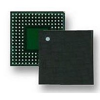
LH7A404N0F000B3 NXP Semiconductors, LH7A404N0F000B3 Datasheet - Page 35

LH7A404N0F000B3
Manufacturer Part Number
LH7A404N0F000B3
Description
MCU ARM9, LCD CTRL, SMD, LFBGA-324
Manufacturer
NXP Semiconductors
Datasheet
1.LH7A404N0F000B3.pdf
(75 pages)
Specifications of LH7A404N0F000B3
Core Size
32bit
No. Of I/o's
64
Ram Memory Size
80KB
Cpu Speed
200MHz
Oscillator Type
External Only
No. Of Timers
3
No. Of Pwm Channels
4
Digital Ic Case Style
LFBGA
Supply Voltage Range
3V
Controller Family/series
LH7A
Peripherals
ADC, DMA, RTC
Rohs Compliant
Yes
Data Bus Width
32 bit
Program Memory Type
ROMLess
Data Ram Size
80 KB
Interface Type
EBI , IrDA , JTAG , PS2 , SCI , UART , USB
Maximum Clock Frequency
200 MHz
Number Of Programmable I/os
64
Number Of Timers
3
Maximum Operating Temperature
+ 85 C
Mounting Style
SMD/SMT
Package / Case
LFBGA
Minimum Operating Temperature
- 40 C
On-chip Adc
10 bit, 9 Channel
Lead Free Status / RoHS Status
Lead free / RoHS Compliant
Available stocks
Company
Part Number
Manufacturer
Quantity
Price
Company:
Part Number:
LH7A404N0F000B3
Manufacturer:
AD
Quantity:
5 742
Company:
Part Number:
LH7A404N0F000B3,55
Manufacturer:
NXP Semiconductors
Quantity:
10 000
32-Bit System-on-Chip
AC Specifications
tions following an internal reference clock signal.
The illustration in Figure 7 represents all cases of
these sets of measurement parameters.
• HCLK, internal System Bus clock (‘C’ in timing data)
• PCLK, the Peripheral Bus clock
• SSPCLK, the Synchronous Serial Port clock
• UARTCLK, the UART Interface clock
• LCDDCLK, the LCD Data clock from the
• ACBITCLK, the AC97 and ACI clock
• SCLK, the Synchronous Memory clock.
point of the clock to the 50 % point of the signal.
Preliminary data sheet
LCD Controller
All signals described in Table 12 relate to transi-
The reference clock signals in this design are:
All signal transitions are measured from the 50 %
REFERENCE
OUTPUT
SIGNAL (O)
INPUT
SIGNAL (I)
CLOCK
Figure 7. LH7A404 Signal Timing
tOVXXX
NXP Semiconductors
represents the amount of time for the output to become
valid from the rising edge of the reference clock signal.
Maximum requirements for tOVXXX are shown in
Table 12.
amount of time the output must be held valid after the
rising edge of the reference clock signal. Minimum
requirements for tOHXXX are listed in Table 12.
amount of setup time the input signal must be valid after
a valid address bus, or rising edge of the peripheral
clock. Maximum requirements for tISXXX are shown in
Table 12.
amount of time the output must be held valid following
the rising edge of the reference clock signal. Minimum
requirements are shown in Table 12.
tISXXX tIHXXX
For outputs from the LH7A404, tOVXXX (e.g. tOVA)
The signal tOHXXX (e.g. tOHA) represents the
For inputs, tISXXX (e.g. tISD) represents the
The signal tIHXXX (e.g. tIHD) represents the
tOHXXX
LH7A404
LH7A404-9
35


