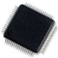
P89LPC9401FBD NXP Semiconductors, P89LPC9401FBD Datasheet - Page 40

P89LPC9401FBD
Manufacturer Part Number
P89LPC9401FBD
Description
IC, MCU 8BIT 80C51, LCD DRIVER, SMD
Manufacturer
NXP Semiconductors
Datasheet
1.P89LPC9401FBD551.pdf
(59 pages)
Specifications of P89LPC9401FBD
Controller Family/series
(8051) 8052
Core Size
8bit
No. Of I/o's
23
Program Memory Size
8KB
Ram Memory Size
256Byte
Cpu Speed
18MHz
Oscillator Type
External, Internal
No. Of Timers
4
No.
RoHS Compliant
Available stocks
Company
Part Number
Manufacturer
Quantity
Price
Part Number:
P89LPC9401FBD
Manufacturer:
NXP/恩智浦
Quantity:
20 000
Company:
Part Number:
P89LPC9401FBD,551
Manufacturer:
NXP Semiconductors
Quantity:
10 000
Company:
Part Number:
P89LPC9401FBD,557
Manufacturer:
NXP Semiconductors
Quantity:
10 000
Company:
Part Number:
P89LPC9401FBDЈ¬551
Manufacturer:
NXP
Quantity:
3 048
Philips Semiconductors
P89LPC9401_1
Preliminary data sheet
7.26.15 I
7.27.1 General description
7.27.2 Features
7.27.3 Flash organization
7.27.4 Using flash as data storage
7.27 Flash program memory
The I
not respond to a read access.
The P89LPC9401 flash memory provides in-circuit electrical erasure and programming.
The flash can be erased, read, and written as bytes. The Sector and Page Erase functions
can erase any flash sector (1 kB) or page (64 bytes). The Chip Erase operation will erase
the entire program memory. ICP using standard commercial programmers is available. In
addition, IAP and byte-erase allows code memory to be used for non-volatile data storage.
On-chip erase and write timing generation contribute to a user-friendly programming
interface. The P89LPC9401 flash reliably stores memory contents even after
100,000 erase and program cycles. The cell is designed to optimize the erase and
programming mechanisms. The P89LPC9401 uses V
the Program/Erase algorithms.
The program memory consists of eight 1 kB sectors on the P89LPC9401 device. Each
sector can be further divided into 64-byte pages. In addition to sector erase, page erase,
and byte erase, a 64-byte page register is included which allows from 1 byte to 64 bytes of
a given page to be programmed at the same time, substantially reducing overall
programming time.
The flash code memory array of this device supports individual byte erasing and
programming. Any byte in the code memory array may be read using the MOVC
instruction, provided that the sector containing the byte has not been secured (a MOVC
instruction is not allowed to read code memory contents of a secured sector). Thus any
byte in a non-secured sector may be used for non-volatile data storage.
2
•
•
•
•
•
•
•
•
•
•
•
C-bus slave addresses
Programming and erase over the full operating voltage range.
Byte erase allows code memory to be used for data storage.
Read/Programming/Erase using ISP/IAP/ICP.
Internal fixed boot ROM, containing low-level IAP routines available to user code.
Default loader providing ISP via the serial port, located in upper end of user program
memory.
Boot vector allows user-provided flash loader code to reside anywhere in the flash
memory space, providing flexibility to the user.
Any flash program or erase operation in 2 ms.
Programming with industry-standard commercial programmers.
Programmable security for the code in the flash for each sector.
100,000 typical erase/program cycles for each byte.
10 year minimum data retention.
2
C-bus slave address is 0111 0000. The LCD controller is a write-only device and will
8-bit two-clock 80C51 microcontroller with 32 segment
Rev. 01 — 5 September 2005
DD
as the supply voltage to perform
© Koninklijke Philips Electronics N.V. 2005. All rights reserved.
P89LPC9401
4 LCD driver
40 of 59


