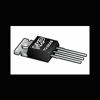
PSMN2R0-30PL NXP Semiconductors, PSMN2R0-30PL Datasheet - Page 6

PSMN2R0-30PL
Manufacturer Part Number
PSMN2R0-30PL
Description
MOSFET,N CH,30V,100A,TO-220AB
Manufacturer
NXP Semiconductors
Datasheet
1.PSMN2R0-30PL127.pdf
(13 pages)
Specifications of PSMN2R0-30PL
Transistor Polarity
N Channel
Drain Source Voltage Vds
30V
On Resistance Rds(on)
1.7mohm
Rds(on) Test Voltage Vgs
20V
Voltage Vgs Max
20V
Operating Temperature Range
-55°C To +175°C
Transistor
RoHS Compliant
Transistor Case Style
TO-220AB
Rohs Compliant
Yes
Available stocks
Company
Part Number
Manufacturer
Quantity
Price
Company:
Part Number:
PSMN2R0-30PL
Manufacturer:
NXP
Quantity:
51 000
Part Number:
PSMN2R0-30PL,127
Manufacturer:
NXP/恩智浦
Quantity:
20 000
NXP Semiconductors
Table 6.
[1]
[2]
PSMN2R0-30PL_1
Product data sheet
Symbol
Source-drain diode
V
t
Q
rr
Fig 5.
Fig 7.
SD
r
Tested to JEDEC standards where applicable.
Measured 3 mm from package.
(A)
(S)
I
g
D
fs
220
165
110
100
55
80
60
40
20
0
0
function of drain-source voltage; typical values
drain current; typical values
Output characteristics: drain current as a
Forward transconductance as a function of
0
0
10
Characteristics
Parameter
source-drain voltage
reverse recovery time
recovered charge
4
3
5
0.5
25
3.5
…continued
50
1
V
GS
Conditions
I
see
I
V
(V) =2.5 V
S
S
DS
1.5
75
= 25 A; V
= 20 A; dI
Figure 16
= 30 V
003aad257
003aad249
V
DS
I
D
(A)
(V)
100
GS
S
2
Rev. 01 — 24 June 2009
/dt = -100 A/µs; V
= 0 V; T
j
= 25 °C;
Fig 6.
Fig 8.
R
(mΩ)
(A)
GS
I
DSon
100
D
80
60
40
20
0
8
6
4
2
0
= 0 V;
function of gate-source voltage; typical values
of gate-source voltage; typical values
Transfer characteristics: drain current as a
Drain source on-state resistance as a function
0
0
N-channel 30 V 2.1 mΩ logic level MOSFET
1
T
j
= 175 °C
5
PSMN2R0-30PL
2
Min
-
-
-
3
Typ
0.76
49
66
25 °C
10
© NXP B.V. 2009. All rights reserved.
V
4
003aad251
GS
003aad254
V
Max
1.2
-
-
GS
(V)
(V)
15
5
Unit
V
ns
nC
6 of 13


