EVAL-AD7747EBZ Analog Devices Inc, EVAL-AD7747EBZ Datasheet - Page 4
EVAL-AD7747EBZ
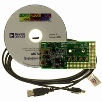
Manufacturer Part Number
EVAL-AD7747EBZ
Description
24-Bit Capacitance-to-Digital Converter Eval. Board
Manufacturer
Analog Devices Inc
Specifications of EVAL-AD7747EBZ
Silicon Manufacturer
Analog Devices
Application Sub Type
Capacitance-to-Digital Converter
Kit Application Type
Data Converter
Silicon Core Number
AD7747
Sensor Type
Touch, Capacitive
Interface
I²C
Voltage - Supply
2.7 V ~ 5.25 V
Embedded
No
Utilized Ic / Part
AD7747
Kit Contents
Board
Rohs Compliant
Yes
Lead Free Status / RoHS Status
Lead free / RoHS Compliant
Sensitivity
-
Sensing Range
-
Lead Free Status / RoHS Status
Lead free / RoHS Compliant, Lead free / RoHS Compliant
Available stocks
Company
Part Number
Manufacturer
Quantity
Price
Company:

Part Number:
EVAL-AD7747EBZ
Manufacturer:
Analog Devices Inc
Quantity:
135


AD7747
Parameter
INTERNAL VOLTAGE REFERENCE
EXTERNAL VOLTAGE REFERENCE INPUT
SERIAL INTERFACE LOGIC INPUTS (SCL, SDA)
OPEN-DRAIN OUTPUT (SDA)
LOGIC OUTPUT ( RDY )
POWER REQUIREMENTS
1
2
3
4
5
6
7
8
9
Capacitance units: 1 pF = 10
Specification is not production tested, but is supported by characterization data at initial product release.
Factory calibrated. The absolute error includes factory gain calibration error, integral nonlinearity error, and offset error after system offset calibration, all at 25°C.
At different temperatures, compensation for gain drift over temperature is required.
The capacitive input offset can be eliminated using a system offset calibration. The accuracy of the system offset calibration is limited by the offset calibration register
LSB size (32 aF) or by converter + system p-p noise during the system capacitive offset calibration, whichever is greater. To minimize the effect of the converter +
system noise, longer conversion times should be used for system capacitive offset calibration. The system capacitance offset calibration range is ±1 pF; the larger
offset can be removed using CAPDACs.
Specification is not production tested, but guaranteed by design.
The gain error is factory calibrated at 25°C. At different temperatures, compensation for gain drift over temperature is required.
The VTCHOP bit in the VT SETUP register must be set to 1 for the specified temperature sensor and voltage input performance.
Using an external temperature sensing diode 2N3906, with nonideality factor n
Full-scale error applies to both positive and negative full scale.
Normal Mode Rejection
Common-Mode Rejection
Voltage
Drift vs. Temperature
Differential REFIN Voltage
Absolute REFIN Voltage
Average REFIN Input Current
Average REFIN Input Current Drift
Common-Mode Rejection
V
V
Hysteresis
Input Leakage Current (SCL)
V
I
V
V
V
V
V
I
I
OH
DD
DD
IH
IL
OL
OL
OH
OL
OH
DD
Input Low Voltage
Output High Leakage Current
Current
Current Power-Down Mode
Input High Voltage
-to-GND Voltage
Output Low Voltage
Output Low Voltage
Output Low Voltage
Output High Voltage
Output High Voltage
−12
2
5
F; 1 fF = 10
2
2
−15
F; 1 aF = 10
Min
1.169
0.1
GND − 0.03
2.1
4.0
V
4.75
2.7
DD
−18
− 0.6
F. Full scale (FS) = 8.192 pF; full-scale range (FSR) = ±8.192 pF.
Typ
75
50
95
1.17
5
2.5
400
±50
80
150
±0.1
0.1
750
700
0.5
Rev. 0 | Page 4 of 28
f
= 1.008, connected as in Figure 37, with total serial resistance <100 Ω.
Max
1.171
V
V
0.8
±1
0.4
1
0.4
0.4
5.25
3.6
850
2
DD
DD
+ 0.03
Unit
dB
dB
dB
V
ppm/°C
V
V
nA/V
pA/V/°C
dB
V
V
mV
μA
V
μA
V
V
V
V
V
V
μA
μA
μA
μA
Test Conditions/Comments
50 Hz ± 1%, conversion time = 122.1 ms
60 Hz ± 1%, conversion time = 122.1 ms
V
T
I
V
I
I
I
I
V
V
Digital inputs equal to V
V
V
Digital inputs equal to V
SINK
SINK
SOURCE
SINK
SOURCE
A
IN
OUT
DD
DD
DD
DD
= 25°C
= 1 V
= 5 V, nominal
= 3.3 V, nominal
= 5 V
= 3.3 V
= −6.0 mA
= 1.6 mA, V
= 100 μA, V
= V
= 200 μA, V
= 100 μA, V
DD
DD
DD
DD
DD
= 5 V
= 3 V
= 5 V
= 3 V
DD
DD
or GND
or GND
Related parts for EVAL-AD7747EBZ
Image
Part Number
Description
Manufacturer
Datasheet
Request
R


Part Number:
Description:
BOARD EVAL FOR SI270X-A
Manufacturer:
Silicon Laboratories Inc
Datasheet:

Part Number:
Description:
BUCK CONV REF DESIGN KIT IP1201
Manufacturer:
International Rectifier
Datasheet:
Part Number:
Description:
BOARD DEMO SYNC DUAL BUCK CNVTER
Manufacturer:
International Rectifier
Datasheet:
Part Number:
Description:
BOARD DEMO SYNC BUCK CONVETER
Manufacturer:
International Rectifier
Datasheet:

Part Number:
Description:
EVALBOARD/EB Omnidirectional microphone - Analog
Manufacturer:
Analog Devices
Datasheet:
Part Number:
Description:
EVALBOARD/EB Omnidirectional microphone - Analog
Manufacturer:
Analog Devices
Datasheet:


Part Number:
Description:
BOARD EVAL LED DRIVER LT3756
Manufacturer:
Linear Technology
Datasheet:

Part Number:
Description:
BOARD EVAL FOR AD7741/7742
Manufacturer:
Analog Devices Inc
Datasheet:

Part Number:
Description:
±1.7g Dual-Axis IMEMS Accelerometer Evaluation Board
Manufacturer:
Analog Devices Inc
Datasheet:

Part Number:
Description:
IC MULTIPLIER ANALOG 8-SOIC T/R
Manufacturer:
Analog Devices Inc
Datasheet:

Part Number:
Description:
IC ANALOG MULTIPLIER 8-DIP
Manufacturer:
Analog Devices Inc
Datasheet:
Part Number:
Description:
IC ANALOG MULTIPLIER 8-SOIC
Manufacturer:
Analog Devices Inc
Datasheet:
Part Number:
Description:
IC ANALOG MULTIPLIER 8-DIP
Manufacturer:
Analog Devices Inc
Datasheet: