EVAL-ADF4360-7EBZ1 Analog Devices Inc, EVAL-ADF4360-7EBZ1 Datasheet - Page 23
EVAL-ADF4360-7EBZ1
Manufacturer Part Number
EVAL-ADF4360-7EBZ1
Description
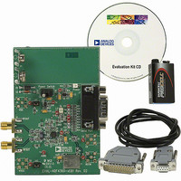
PLL/Frequency Synthesizer EVAL BOARD
Manufacturer
Analog Devices Inc
Datasheet
1.ADF4360-7BCPZ.pdf
(28 pages)
Specifications of EVAL-ADF4360-7EBZ1
Silicon Manufacturer
Analog Devices
Application Sub Type
Integer-N Synthesizer
Kit Application Type
Clock & Timing
Silicon Core Number
ADF4360-7
Kit Contents
Board
Main Purpose
Timing, Frequency Synthesizer
Embedded
No
Utilized Ic / Part
ADF4360-7
Primary Attributes
Single Integer-N PLL with VCO
Secondary Attributes
900MHz, 200kHz PFD
Frequency
1.8GHz
Rohs Compliant
Yes
Lead Free Status / RoHS Status
Lead free / RoHS Compliant
Other names
EVAL-ADF4360-7EB1
EVAL-ADF4360-7EB1
Q5173330
Q5652985
EVAL-ADF4360-7EB1
Q5173330
Q5652985


INTERFACING
The ADF4360 family has a simple SPI®-compatible serial inter-
face for writing to the device. CLK, DATA, and LE control the
data transfer. When LE goes high, the 24 bits that have been
clocked into the appropriate register on each rising edge of CLK
are transferred to the appropriate latch. See Figure 2 for the
timing diagram and Table 5 for the latch truth table.
The maximum allowable serial clock rate is 20 MHz. This
means that the maximum update rate possible is 833 kHz or
one update every 1.2 µs. This is certainly more than adequate
for systems that have typical lock times in hundreds of micro-
seconds.
ADuC812 Interface
Figure 27 shows the interface between the ADF4360 family and
the ADuC812 MicroConverter®. Because the ADuC812 is based
on an 8051 core, this interface can be used with any 8051-based
microcontroller. The MicroConverter is set up for SPI master
mode with CPHA = 0. To initiate the operation, the I/O port
driving LE is brought low. Each latch of the ADF4360 family
needs a 24-bit word, which is accomplished by writing three
8-bit bytes from the MicroConverter to the device. After the
third byte has been written, the LE input should be brought
high to complete the transfer.
I/O port lines on the ADuC812 are also used to control power-
down (CE input) and detect lock (MUXOUT configured as lock
detect and polled by the port input). When operating in the
described mode, the maximum SCLOCK rate of the ADuC812
is 4 MHz. This means that the maximum rate at which the out-
put frequency can be changed is 166 kHz.
ADuC812
I/O PORTS
SCLOCK
Figure 27. ADuC812 to ADF4360-x Interface
MOSI
SCLK
SDATA
CE
MUXOUT
(LOCK DETECT)
LE
ADF4360-x
Rev. A | Page 23 of 28
ADSP-2181 Interface
Figure 28 shows the interface between the ADF4360 family and
the ADSP-21xx digital signal processor. The ADF4360 family
needs a 24-bit serial word for each latch write. The easiest way
to accomplish this using the ADSP-21xx family is to use the
autobuffered transmit mode of operation with alternate fram-
ing. This provides a means for transmitting an entire block of
serial data before an interrupt is generated.
Set up the word length for 8 bits and use three memory loca-
tions for each 24-bit word. To program each 24-bit latch, store
the 8-bit bytes, enable the autobuffered mode, and write to the
transmit register of the DSP. This last operation initiates the
autobuffer transfer.
PCB DESIGN GUIDELINES FOR CHIP SCALE PACKAGE
The leads on the chip scale package (CP-24) are rectangular.
The printed circuit board pad for these should be 0.1 mm
longer than the package lead length and 0.05 mm wider than
the package lead width. The lead should be centered on the pad
to ensure that the solder joint size is maximized.
The bottom of the chip scale package has a central thermal pad.
The thermal pad on the printed circuit board should be at least
as large as this exposed pad. On the printed circuit board, there
should be a clearance of at least 0.25 mm between the thermal
pad and the inner edges of the pad pattern to ensure that short-
ing is avoided.
Thermal vias may be used on the printed circuit board thermal
pad to improve thermal performance of the package. If vias
are used, they should be incorporated into the thermal pad at a
1.2 mm pitch grid. The via diameter should be between 0.3 mm
and 0.33 mm, and the via barrel should be plated with 1 ounce
of copper to plug the via.
The user should connect the printed circuit thermal pad to
AGND. This is internally connected to AGND.
ADSP-21xx
I/O PORTS
Figure 28. ADSP-21xx to ADF4360-x Interface
SCLOCK
MOSI
TFS
SDATA
SCLK
CE
MUXOUT
(LOCK DETECT)
LE
ADF4360-x
ADF4360-7
Related parts for EVAL-ADF4360-7EBZ1
Image
Part Number
Description
Manufacturer
Datasheet
Request
R

Part Number:
Description:
±1.7g Dual-Axis IMEMS Accelerometer Evaluation Board
Manufacturer:
Analog Devices Inc
Datasheet:

Part Number:
Description:
Inertial Sensor Evaluation System
Manufacturer:
Analog Devices Inc
Datasheet:
Part Number:
Description:
Manufacturer:
Analog Devices Inc
Datasheet:
Part Number:
Description:
Manufacturer:
Analog Devices Inc
Datasheet:
Part Number:
Description:
Manufacturer:
Analog Devices Inc
Datasheet:
Part Number:
Description:
Manufacturer:
Analog Devices Inc
Datasheet:
Part Number:
Description:
Manufacturer:
Analog Devices Inc
Datasheet:
Part Number:
Description:
Manufacturer:
Analog Devices Inc
Datasheet:
Part Number:
Description:
Manufacturer:
Analog Devices Inc
Datasheet:
Part Number:
Description:
Manufacturer:
Analog Devices Inc
Datasheet:
Part Number:
Description:
Manufacturer:
Analog Devices Inc
Datasheet:
Part Number:
Description:
Manufacturer:
Analog Devices Inc
Datasheet:
Part Number:
Description:
Manufacturer:
Analog Devices Inc
Datasheet: