EVAL-ADF4360-7EBZ1 Analog Devices Inc, EVAL-ADF4360-7EBZ1 Datasheet - Page 4
EVAL-ADF4360-7EBZ1
Manufacturer Part Number
EVAL-ADF4360-7EBZ1
Description
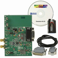
PLL/Frequency Synthesizer EVAL BOARD
Manufacturer
Analog Devices Inc
Datasheet
1.ADF4360-7BCPZ.pdf
(28 pages)
Specifications of EVAL-ADF4360-7EBZ1
Silicon Manufacturer
Analog Devices
Application Sub Type
Integer-N Synthesizer
Kit Application Type
Clock & Timing
Silicon Core Number
ADF4360-7
Kit Contents
Board
Main Purpose
Timing, Frequency Synthesizer
Embedded
No
Utilized Ic / Part
ADF4360-7
Primary Attributes
Single Integer-N PLL with VCO
Secondary Attributes
900MHz, 200kHz PFD
Frequency
1.8GHz
Rohs Compliant
Yes
Lead Free Status / RoHS Status
Lead free / RoHS Compliant
Other names
EVAL-ADF4360-7EB1
EVAL-ADF4360-7EB1
Q5173330
Q5652985
EVAL-ADF4360-7EB1
Q5173330
Q5652985


ADF4360-7
Parameter
RF OUTPUT CHARACTERISTICS
NOISE CHARACTERISTIC
1
2
3
4
5
6
7
8
9
10
11
12
13
Operating temperature range is –40°C to +85°C.
Guaranteed by design. Sample tested to ensure compliance.
I
T
Unless otherwise stated, these characteristics are guaranteed for VCO core power = 5 mA. L1, L2 = 13 nH, 470 Ω resistors to GND in parallel with L1, L2.
Jumping from 490 MHz to 585 MHz. PFD frequency = 200 kHz; loop bandwidth = 10 kHz.
Using 50 Ω resistors to V
The noise of the VCO is measured in open-loop conditions.
The synthesizer phase-noise floor is estimated by measuring the in-band phase noise at the output of the VCO and subtracting 20 log N (where N is the N divider value).
CP
The phase noise is measured with the EVAL-ADF4360-xEB1 Evaluation Board and the HP 8562E Spectrum Analyzer. The Spectrum Analyzer provides the REF
f
f
The spurious signals are measured with the EVAL-ADF4360-xEB1 Evaluation Board and the HP 8562E Spectrum Analyzer. The Spectrum Analyzer provides the REF
for the synthesizer; f
synthesizer; offset frequency = 1 kHz.
A
REFIN
REFIN
Maximum VCO Output Frequency
Minimum VCO Output Frequency
VCO Output Frequency
VCO Frequency Range
VCO Sensitivity
Lock Time
Frequency Pushing (Open Loop)
Frequency Pulling (Open Loop)
Harmonic Content (Second)
Harmonic Content (Third)
Output Power
Output Power Variation
VCO Tuning Range
VCO Phase-Noise Performance
Synthesizer Phase-Noise Floor
In-Band Phase Noise
RMS Integrated Phase Error
Spurious Signals due to PFD
Level of Unlocked Signal with
= 25°C; AV
is internally modified to maintain constant loop gain over the frequency range.
Frequency
MTLD Enabled
= 10 MHz; f
= 10 MHz; f
DD
6
= DV
PFD
PFD
11, 13
5, 7
= 200 kHz; N = 2500; loop B/W = 10 kHz.
= 1 MHz; N = 500; loop B/W = 25 kHz.
DD
REFOUT
= V
VCO
10, 11
VCO
= 10 MHz @ 0 dBm.
, into a 50 Ω load. For tuned loads, see the Output M
5
= 3.3 V; P = 32.
12
5
9
8
490/585
1.25/2.5
B Version
1800
350
1.2
12
400
6
15
−19
−9
−14/−5
±3
−116
−138
−144
−148
−172
−163
−147
−92
0.3
−70
−44
MHz min/max
V min/max
Unit
MHz
MHz
Ratio
MHz/V typ
µs typ
MHz/V typ
kHz typ
dBc typ
dBc typ
dBm typ
dB typ
dBc/Hz typ
dBc/Hz typ
dBc/Hz typ
dBc/Hz typ
dBc/Hz typ
dBc/Hz typ
dBc/Hz typ
dBc/Hz typ
Degrees typ
dBc typ
dBm typ
Rev. A | Page 4 of 28
atching
section.
Conditions/Comments
I
Inductance Value section.
L1, L2 = 13 nH. See the Choosing the Correct Inductance Value
section for other frequency values.
F
L1, L2 = 13 nH. See the Choosing the Correct Inductance Value
section for other sensitivity values.
To within 10 Hz of final frequency.
Into 2.00 VSWR load.
Programmable in 3 dB steps. See Table 7.
For tuned loads, see Output Matching section.
@ 100 kHz offset from carrier.
@ 1 MHz offset from carrier.
@ 3 MHz offset from carrier.
@ 10 MHz offset from carrier.
@ 25 kHz PFD frequency.
@ 200 kHz PFD frequency.
@ 8 MHz PFD frequency.
@ 1 kHz offset from carrier.
100 Hz to 100 kHz.
CORE
MAX
/F
= 5 mA. Depending on L. See the Choosing the Correct
MIN
IN
for the
IN
Related parts for EVAL-ADF4360-7EBZ1
Image
Part Number
Description
Manufacturer
Datasheet
Request
R

Part Number:
Description:
±1.7g Dual-Axis IMEMS Accelerometer Evaluation Board
Manufacturer:
Analog Devices Inc
Datasheet:

Part Number:
Description:
Inertial Sensor Evaluation System
Manufacturer:
Analog Devices Inc
Datasheet:
Part Number:
Description:
Manufacturer:
Analog Devices Inc
Datasheet:
Part Number:
Description:
Manufacturer:
Analog Devices Inc
Datasheet:
Part Number:
Description:
Manufacturer:
Analog Devices Inc
Datasheet:
Part Number:
Description:
Manufacturer:
Analog Devices Inc
Datasheet:
Part Number:
Description:
Manufacturer:
Analog Devices Inc
Datasheet:
Part Number:
Description:
Manufacturer:
Analog Devices Inc
Datasheet:
Part Number:
Description:
Manufacturer:
Analog Devices Inc
Datasheet:
Part Number:
Description:
Manufacturer:
Analog Devices Inc
Datasheet:
Part Number:
Description:
Manufacturer:
Analog Devices Inc
Datasheet:
Part Number:
Description:
Manufacturer:
Analog Devices Inc
Datasheet:
Part Number:
Description:
Manufacturer:
Analog Devices Inc
Datasheet: