EA-QSB-103 Embedded Artists, EA-QSB-103 Datasheet - Page 17
EA-QSB-103
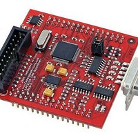
Manufacturer Part Number
EA-QSB-103
Description
MCU, MPU & DSP Development Tools QUICKSTART PROTOTYPE BRD W/ LPC2129 CAN
Manufacturer
Embedded Artists
Specifications of EA-QSB-103
Processor To Be Evaluated
LPC2129
Data Bus Width
16 bit, 32 bit
Interface Type
RS-232, CAN, I2C, SPI, UART
Core
ARM7TDMI-S
Dimensions
55 mm x 58 mm
Maximum Operating Temperature
+ 85 C
Operating Supply Voltage
5 V
Lead Free Status / RoHS Status
Lead free / RoHS Compliant


NXP Semiconductors
Product data sheet
LPC2109_2119_2129_6
6.12.1 Features
6.12.2 Features available in LPC2109/2119/2129/01 only
6.13.1 Features
6.12 SPI serial I/O controller
6.13 SSP controller (LPC2109/2119/2129/01 only)
6.14 General purpose timers
The LPC2109/2119/2129 each contain two SPIs. The SPI is a full duplex serial interface,
designed to be able to handle multiple masters and slaves connected to a given bus. Only
a single master and a single slave can communicate on the interface during a given data
transfer. During a data transfer the master always sends a byte of data to the slave, and
the slave always sends a byte of data to the master.
Remark: This peripheral is available in LPC2109/2119/2129/01 only.
The SSP is a controller capable of operation on a SPI, 4-wire SSI, or Microwire bus. It can
interact with multiple masters and slaves on the bus. Only a single master and a single
slave can communicate on the bus during a given data transfer. Data transfers are in
principle full duplex, with frames of four to 16 bits of data flowing from the master to the
slave and from the slave to the master.
While the SSP and SPI1 peripherals share the same physical pins, it is not possible to
have both of these two peripherals active at the same time. Application can switch on the
fly from SPI1 to SSP and back.
The Timer/Counter is designed to count cycles of the peripheral clock (PCLK) or an
externally supplied clock and optionally generate interrupts or perform other actions at
specified timer values, based on four match registers. It also includes four capture inputs
•
•
•
•
•
•
•
•
•
•
•
Compliant with Serial Peripheral Interface (SPI) specification.
Synchronous, Serial, Full Duplex communication.
Combined SPI master and slave.
Maximum data bit rate of
Eight to 16 bits per frame.
When the SPI interface is used in Master mode, the SSELn pin is not needed (can be
used for a different function).
Compatible with Motorola’s SPI, Texas Instrument’s 4-wire SSI, and National
Semiconductor’s Microwire buses.
Synchronous serial communication.
Master or slave operation.
8-frame FIFOs for both transmit and receive.
Four to 16 bits per frame.
Rev. 06 — 10 December 2007
1
8
of the input clock rate.
LPC2109/2119/2129
Single-chip 16/32-bit microcontrollers
© NXP B.V. 2007. All rights reserved.
17 of 44
Related parts for EA-QSB-103
Image
Part Number
Description
Manufacturer
Datasheet
Request
R

Part Number:
Description:
MCU, MPU & DSP Development Tools QUICKSTART PROTOTYPE BRD
Manufacturer:
Embedded Artists
Datasheet:

Part Number:
Description:
MCU, MPU & DSP Development Tools LPC2148 USB QUICKSTART BRD
Manufacturer:
Embedded Artists
Datasheet:

Part Number:
Description:
MCU, MPU & DSP Development Tools QUICKSTART PROTOTYPE BRD W/ LPC2106 RS232
Manufacturer:
Embedded Artists
Datasheet:

Part Number:
Description:
MCU, MPU & DSP Development Tools LPC2129 CAN QUICKSTART BRD
Manufacturer:
Embedded Artists
Datasheet:
Part Number:
Description:
MCU, MPU & DSP Development Tools QUICKSTART PROTOTYPE BRD W/ LPC2148
Manufacturer:
Embedded Artists
Datasheet:
Part Number:
Description:
MCU, MPU & DSP Development Tools LPC2106 RS232 QUICKSTART BRD
Manufacturer:
Embedded Artists
Datasheet:

Part Number:
Description:
BOARD QUICK START LPC1343
Manufacturer:
Embedded Artists
Datasheet:

Part Number:
Description:
Development Boards & Kits - ARM QUICK START BOARD LPC11U35
Manufacturer:
Embedded Artists
Datasheet:
Part Number:
Description:
KIT LPC3141 SODIMM 66X48 200POS
Manufacturer:
Embedded Artists
Datasheet:
Part Number:
Description:
KIT LPC3152 SODIMM 66X48 200POS
Manufacturer:
Embedded Artists
Datasheet:
Part Number:
Description:
BOARD OEM W/LPC2478 MCU
Manufacturer:
Embedded Artists
Datasheet:
Part Number:
Description:
KIT LPC3250 259 WITH QVGA
Manufacturer:
Embedded Artists
Datasheet: