EA-QSB-103 Embedded Artists, EA-QSB-103 Datasheet - Page 8
EA-QSB-103
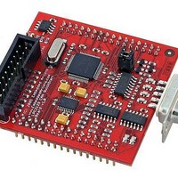
Manufacturer Part Number
EA-QSB-103
Description
MCU, MPU & DSP Development Tools QUICKSTART PROTOTYPE BRD W/ LPC2129 CAN
Manufacturer
Embedded Artists
Specifications of EA-QSB-103
Processor To Be Evaluated
LPC2129
Data Bus Width
16 bit, 32 bit
Interface Type
RS-232, CAN, I2C, SPI, UART
Core
ARM7TDMI-S
Dimensions
55 mm x 58 mm
Maximum Operating Temperature
+ 85 C
Operating Supply Voltage
5 V
Lead Free Status / RoHS Status
Lead free / RoHS Compliant


NXP Semiconductors
Table 3.
Product data sheet
LPC2109_2119_2129_6
Symbol
P1[16]/
TRACEPKT0
P1[17]/
TRACEPKT1
P1[18]/
TRACEPKT2
P1[19]/
TRACEPKT3
P1[20]/
TRACESYNC
P1[21]/
PIPESTAT0
P1[22]/
PIPESTAT1
P1[23]/
PIPESTAT2
P1[24]/
TRACECLK
P1[25]/EXTIN0
P1[26]/RTCK
P1[27]/TDO
P1[28]/TDI
P1[29]/TCK
P1[30]/TMS
P1[31]/TRST
TD1
RESET
XTAL1
XTAL2
V
V
V
V
SS
SSA
SSA(PLL)
DD(1V8)
Pin description
Pin
16
12
8
4
48
44
40
36
32
28
24
64
60
56
52
20
10
57
62
61
6, 18, 25,
42, 50
59
58
17, 49
…continued
Type Description
O
O
O
O
O
O
O
O
O
I
I/O
O
I
I
I
I
O
I
I
O
I
I
I
I
Trace Packet, bit 0. Standard I/O port with internal pull-up.
Trace Packet, bit 1. Standard I/O port with internal pull-up.
Trace Packet, bit 2. Standard I/O port with internal pull-up.
Trace Packet, bit 3. Standard I/O port with internal pull-up.
Trace Synchronization. Standard I/O port with internal pull-up.
Note: LOW on this pin while RESET is LOW, enables pins P1[25:16] to operate as
Trace port after reset.
Pipeline Status, bit 0. Standard I/O port with internal pull-up.
Pipeline Status, bit 1. Standard I/O port with internal pull-up.
Pipeline Status, bit 2. Standard I/O port with internal pull-up.
Trace Clock. Standard I/O port with internal pull-up.
External Trigger Input. Standard I/O with internal pull-up.
Returned Test Clock output. Extra signal added to the JTAG port. Assists debugger
synchronization when processor frequency varies. Bidirectional pin with internal
pull-up.
Note: LOW on this pin while RESET is LOW, enables pins P1[31:26] to operate as
Debug port after reset.
Test Data out for JTAG interface.
Test Data in for JTAG interface.
Test Clock for JTAG interface. This clock must be slower than
(CCLK) for the JTAG interface to operate.
Test Mode Select for JTAG interface.
Test Reset for JTAG interface.
CAN1 transmitter output.
External reset input; a LOW on this pin resets the device, causing I/O ports and
peripherals to take on their default states, and processor execution to begin at
address 0. TTL with hysteresis, 5 V tolerant.
Input to the oscillator circuit and internal clock generator circuits.
Output from the oscillator amplifier.
Ground: 0 V reference.
Analog ground; 0 V reference. This should nominally be the same voltage as V
but should be isolated to minimize noise and error.
PLL analog ground; 0 V reference. This should nominally be the same voltage as
V
1.8 V core power supply; this is the power supply voltage for internal circuitry.
SS
, but should be isolated to minimize noise and error.
Rev. 06 — 10 December 2007
LPC2109/2119/2129
Single-chip 16/32-bit microcontrollers
1
6
© NXP B.V. 2007. All rights reserved.
of the CPU clock
8 of 44
SS
,
Related parts for EA-QSB-103
Image
Part Number
Description
Manufacturer
Datasheet
Request
R

Part Number:
Description:
MCU, MPU & DSP Development Tools QUICKSTART PROTOTYPE BRD
Manufacturer:
Embedded Artists
Datasheet:

Part Number:
Description:
MCU, MPU & DSP Development Tools LPC2148 USB QUICKSTART BRD
Manufacturer:
Embedded Artists
Datasheet:

Part Number:
Description:
MCU, MPU & DSP Development Tools QUICKSTART PROTOTYPE BRD W/ LPC2106 RS232
Manufacturer:
Embedded Artists
Datasheet:

Part Number:
Description:
MCU, MPU & DSP Development Tools LPC2129 CAN QUICKSTART BRD
Manufacturer:
Embedded Artists
Datasheet:
Part Number:
Description:
MCU, MPU & DSP Development Tools QUICKSTART PROTOTYPE BRD W/ LPC2148
Manufacturer:
Embedded Artists
Datasheet:
Part Number:
Description:
MCU, MPU & DSP Development Tools LPC2106 RS232 QUICKSTART BRD
Manufacturer:
Embedded Artists
Datasheet:

Part Number:
Description:
BOARD QUICK START LPC1343
Manufacturer:
Embedded Artists
Datasheet:

Part Number:
Description:
Development Boards & Kits - ARM QUICK START BOARD LPC11U35
Manufacturer:
Embedded Artists
Datasheet:
Part Number:
Description:
KIT LPC3141 SODIMM 66X48 200POS
Manufacturer:
Embedded Artists
Datasheet:
Part Number:
Description:
KIT LPC3152 SODIMM 66X48 200POS
Manufacturer:
Embedded Artists
Datasheet:
Part Number:
Description:
BOARD OEM W/LPC2478 MCU
Manufacturer:
Embedded Artists
Datasheet:
Part Number:
Description:
KIT LPC3250 259 WITH QVGA
Manufacturer:
Embedded Artists
Datasheet: