CYIS1SM1000-EVAL Cypress Semiconductor Corp, CYIS1SM1000-EVAL Datasheet - Page 16
CYIS1SM1000-EVAL
Manufacturer Part Number
CYIS1SM1000-EVAL
Description
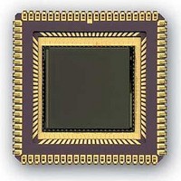
MCU, MPU & DSP Development Tools 1M Pixel Radiation Hard CMOS Img Snsr
Manufacturer
Cypress Semiconductor Corp
Datasheet
1.CYIS1SM1000-EVAL.pdf
(24 pages)
Specifications of CYIS1SM1000-EVAL
Lead Free Status / RoHS Status
Lead free / RoHS Compliant


Cypress Semiconductor Corporation 3901 North First Street
Contact:
Pin
28
29
30
31
32
33
34
35
36
37
38
39
40
41
42
43
44
45
46
47
48
49
50
51
52
53
54
STAR-1000
Datasheet
Pin name
G0
CAL
OUT
BLACKREF
VDDA
VDDD
GNDA
GNDD
NBIAS_ARRAY
TESTPIX_OUT
TESTPIX_RESET
n.c.
n.c.
n.c.
n.c.
n.c.
n.c.
n.c.
n.c.
n.c.
TESTPIXARRAY
PHOTODIODE
NBIAS_ANA
NBIAS_ANA2
IN_ADC
VDD_ADC_ANA
GND_ADC_ANA
info@Fillfactory.com
Pin type
Input
Input
Output
Input
Supply
Supply
Ground
Ground
Input
Output
Input
Output
Output
Input
Input
Input
Supply
Ground
Document #:38-05714 Rev.**(Revision 6.5)
Pin description
LSB; G1 = MSB (‘00’ = unity gain; ‘01’ = x2; ‘10’= x4;
‘11’=x8).
Digital input (active high). Initialization of output
amplifier. Output amplifier will output BLACKREF in
unity gain mode when CAL is high (1).
Apply pulse pattern (see sensor timing diagram).
Analog output video signal.
To be connected to the analog input of the internal (pin
52) 10-bit ADC or an external ADC.
Analog input. Control voltage for output signal offset
level.
Buffered on-chip, the reference level can be generated by
a 100kΩ resistive divider. Connect to 2 V DC for use
with on-chip ADC.
Analog power supply of image core (typical 5 V).
Digital power supply of image core (typical 5V).
Analog ground of image core.
Digital ground of image core.
Analog input. Biasing of the pixel array.
Connect with 1MΩ to VDDA and decouple with 100 nF
capacitor to GND.
Output of single test pixel. Can be used for electro-
optical evaluation.
Digital input (active high). Reset signal of single test
pixel. Used to reset the single test pixel during electro-
optical evaluation.
Analog output of an array of 20 x 35 test pixels where all
photodiodes are connected in parallel. Can be used for
electro-optical evaluation.
Plain photo diode (without circuitry). Area of the
photodiode = 20 x 35 pixels. Can be used for electro-
optical evaluation.
Analog input. Analog biasing of the ADC circuitry.
Connect with 100kΩ to VDDA and decouple with 100nF
to GND.
Analog input of the internal ADC. Connect to analog
output of image sensor (pin 30).
Input range (typically 2V and 4V) of the internal ADC is
set between by VLOW_ADC (pin 55) and
VHIGH_ADC (pin 62).
Analog power supply of the ADC (typical 5V).
Analog ground of the ADC.
San Jose, CA 95134 408-943-2600
Page 16 of 24
Related parts for CYIS1SM1000-EVAL
Image
Part Number
Description
Manufacturer
Datasheet
Request
R

Part Number:
Description:
Manufacturer:
Cypress Semiconductor Corp
Datasheet:
Part Number:
Description:
Manufacturer:
Cypress Semiconductor Corp
Datasheet:
Part Number:
Description:
Manufacturer:
Cypress Semiconductor Corp
Datasheet:
Part Number:
Description:
Manufacturer:
Cypress Semiconductor Corp
Datasheet:
Part Number:
Description:
Manufacturer:
Cypress Semiconductor Corp
Datasheet: