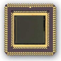
CYIS1SM1000-EVAL Cypress Semiconductor Corp, CYIS1SM1000-EVAL Datasheet - Page 6

CYIS1SM1000-EVAL
Manufacturer Part Number
CYIS1SM1000-EVAL
Description
MCU, MPU & DSP Development Tools 1M Pixel Radiation Hard CMOS Img Snsr
Manufacturer
Cypress Semiconductor Corp
Datasheet
1.CYIS1SM1000-EVAL.pdf
(24 pages)
Specifications of CYIS1SM1000-EVAL
Lead Free Status / RoHS Status
Lead free / RoHS Compliant
The Y-decoder logic has two different reset inputs: “RESET” and “RESET_DS”.
Activation of “RESET” will reset the pixel to the Vdd level; activation of
“RESET_DS” will reset the pixel to the voltage level on the “VREF” input. This
feature allows the application of the so-called dual slope integration (see APPENDIX
B).
“RESET_DS” must never be activated.
All outputs from the pixels in a column are connected in parallel to a column
amplifier. This amplifier samples the output voltage and the reset level of the pixel
whose row is selected at that moment and presents these voltage levels to the output
amplifier. As a result the pixels are always reset immediately after read-out as part of
the sample procedure and the maximum integration time of a pixel is the time
between two read cycles.
The output amplifier combines subtraction of pixel signal level from reset level with a
programmable gain amplifier. Since the amplifier is AC coupled it also contains a
provision to maintain and restore the proper DC level.
An analogue signal multiplexer feeds the pixel signal to the final unity gain buffer to
provide the required drive capability. Apart from the pixel signal also three other
external analogue signals can be fed to the output buffer. All these signals can be
digitalised by the on-chip ADC if the output of this buffer is externally connected to
the input of the ADC.
The purpose of the additional analogue inputs (“A_IN1”, “A_IN2” and “A_IN3”) is
to allow a possibility to process other analogue signals through the image sensors
signal path. These signals can thus be converted by the ADC and processed by the
image controller FPGA.
frequency or DC signals and have a reduced bandwidth, compared with the image
signal path.
The image sensor has a 10-bit ADC that is electrically separated from the rest of the
image sensor circuits and can be powered down if an external ADC is used. The
conversion takes place at the falling edge of the clock and the output pins can be
disabled to allow operation of the device in a bus structure.
Cypress Semiconductor Corporation 3901 North First Street
Contact:
1.3.
1.4.
1.5.
If dual slope integration is not needed “VREF” can be tied to Vdd and
STAR-1000
Datasheet
info@Fillfactory.com
The column amplifiers
The output amplifier and analog multiplexer
The ADC
Document #:38-05714 Rev.**(Revision 6.5)
The additional analogue inputs are intended for low
San Jose, CA 95134 408-943-2600
Page 6 of 24


