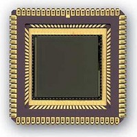
CYIS1SM1000-EVAL Cypress Semiconductor Corp, CYIS1SM1000-EVAL Datasheet - Page 17

CYIS1SM1000-EVAL
Manufacturer Part Number
CYIS1SM1000-EVAL
Description
MCU, MPU & DSP Development Tools 1M Pixel Radiation Hard CMOS Img Snsr
Manufacturer
Cypress Semiconductor Corp
Datasheet
1.CYIS1SM1000-EVAL.pdf
(24 pages)
Specifications of CYIS1SM1000-EVAL
Lead Free Status / RoHS Status
Lead free / RoHS Compliant
Cypress Semiconductor Corporation 3901 North First Street
Contact:
Pin
55
56
57
58
59
60
61
62
63
64
65
66
67
68
69
70
71
72
73
74
75
76
77
78
79
80
81
STAR-1000
Datasheet
Pin name
VLOW_ADC
n.c.
PBIASDIG2
BITINVERT
TRI_ADC
D0
CLK
VHIGH_ADC
GND_ADC_ANA
VDD_ADC_ANA
VDD_ADC_DIG
GND_ADC_DIG
VDD_DIG_OUT
D1
D2
D3
D4
D5
VDDA
GNDA
GND_AB
VREF
VRES
D6
D7
D8
D9
info@Fillfactory.com
Pin type
Input
Input
Input
Input
Input
Input
Input
Ground
Supply
Supply
Output
Supply
Output
Output
Output
Output
Output
Supply
Ground
Supply
Supply
Supply
Output
Output
Output
Output
Document #:38-05714 Rev.**(Revision 6.5)
Pin description
Low reference voltage of internal ADC. Nominal input
range of the ADC is between 2V and 4V. The resistance
between VLOW_ADC and VHIGH_ADC is about 1.5
kΩ.
Connect with 1k5Ω to GND and decouple with 100nF to
GND.
Connect with 20K to GND and decouple with 100nF to
VDDA.
Digital input. Inversion of the ADC output bits. 0 =
invert output bits (0 => black: 1023; white: 0), 1 = no
inversion of output bits (black: 0; white: 1023).
Digital input. Tri-state control of digital ADC outputs (1
= tri-state; 0 = normal mode).
ADC output bits.
D0 = LSB, D9=MSB.
Digital input. ADC clock. ADC converts on falling edge.
High reference voltage of internal ADC. Nominal input
range of the ADC is between 2V and 4V. The resistance
between VLOW_ADC and VHIGH_ADC is about 1.5
kΩ.
Connect with 1k1Ω to VDDA and decouple with 100nF
to GND.
Analog ground of the ADC circuitry.
Analog supply of the ADC circuitry (typical 5V).
Digital supply of the ADC circuitry (typical 5V).
Digital ground of the ADC circuitry.
Power supply of ADC digital output. Connect to 5V for
or normal operation. Can be brought to lower voltage
when image sensor must be interfaced to low voltage
periphery.
ADC output bits.
D0 = LSB, D9=MSB.
Analog supply of the image core (typical 5V).
Analog ground of the image core (typical 5V).
Anti-blooming drain control voltage. Default: connect to
ground, the anti-blooming is operational but not
maximal. Apply 1 V DC for improved anti-blooming.
Analog supply. Reset level for RESET_DS. Can be used
for extended optical dynamic range. See FAQ for more
details.
Analog supply. Reset level for RESET (typical 5V).
ADC output bits.
D0 = LSB, D9=MSB.
San Jose, CA 95134 408-943-2600
Page 17 of 24


