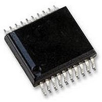
TDA8542TS/N1 NXP Semiconductors, TDA8542TS/N1 Datasheet - Page 8

TDA8542TS/N1
Manufacturer Part Number
TDA8542TS/N1
Description
AMP, AUDIO, PWR, 1.2W, AB, 20SSOP
Manufacturer
NXP Semiconductors
Datasheet
1.TDA8542TSN1.pdf
(20 pages)
Specifications of TDA8542TS/N1
Amplifier Class
AB
No. Of Channels
2
Output Power
1.2W
Load Impedance
16ohm
Operating Temperature Range
-40°C To +85°C
Amplifier Case Style
SSOP
No. Of Pins
20
Base Number
8542
Supply Voltage Range
2.2V To 18V
Thd + N
0.15% @ 0.4W, 8ohm, VCC=5V
Rohs Compliant
Yes
Lead Free Status / RoHS Status
Lead free / RoHS Compliant
Available stocks
Company
Part Number
Manufacturer
Quantity
Price
Company:
Part Number:
TDA8542TS/N1
Manufacturer:
PION
Quantity:
4 015
Philips Semiconductors
TEST AND APPLICATION INFORMATION
Test conditions
Because the application can be either Bridge-Tied Load
(BTL) or Single-Ended (SE), the curves of each application
are shown separately.
The thermal resistance = 110 K/W for the SSOP20; the
maximum sine wave power dissipation for T
For T
Thermal design considerations
The ‘measured’ thermal resistance of the IC package is
highly dependent on the configuration and size of the
application board. Data may not be comparable between
different semiconductor manufacturers because the
application boards and test methods are not (yet)
standardized. Also, the thermal performance of packages
for a specific application may be different than presented
here, because the configuration of the application boards
(copper area) may be different. Philips Semiconductors
uses FR-4 type application boards with 1 oz copper traces
with solder coating.
The SSOP package has improved thermal conductivity
which reduces the thermal resistance. Using a practical
PCB layout (see Fig.22) with wider copper tracks to the
corner pins and just under the IC, the thermal resistance
from junction to ambient can be reduced to approximately
80 K/W. For T
dissipation for this PCB layout is:
BTL application
T
f = 1 kHz, R
22 Hz to 22 kHz.
The BTL application diagram is illustrated in Fig.3.
The quiescent current has been measured without any
load impedance. The total harmonic distortion as a
1998 Mar 25
150 25
--------------------- -
150 60
--------------------- -
amb
2
110
110
–
–
= 25 C if not specially mentioned, V
amb
0.7 W BTL audio amplifier
= 60 C the maximum total power dissipation is:
=
=
L
1.14 W
0.82 W
= 8 , G
amb
= 60 C the maximum total power
v
= 20 dB, audio band-pass
150 60
--------------------- -
80
–
CC
amb
=
= 5 V,
1.12 W
= 25 C is:
8
function of frequency was measured with a low-pass filter
of 80 kHz. The value of capacitor C3 influences the
behaviour of the SVRR at low frequencies, increasing the
value of C3 increases the performance of the SVRR.
The figure of the mode select voltage (V
of the supply voltage shows three areas; operating, mute
and standby. It shows, that the DC-switching levels of the
mute and standby respectively depends on the supply
voltage level.
SE application
T
f = 1 kHz, R
22 Hz to 22 kHz.
The SE application diagram is illustrated in Fig.14.
If the BTL/SE pin (pin 6) is connected to ground, the
positive outputs (pins 3 and 8) will be in mute condition
with a DC level of
(R
without output coupling capacitors; load between negative
output and one of the positive outputs (e.g. pin 3) as
common pin. The channel separation will be less in
comparison with the application using a coupling capacitor
connected to ground.
Increasing the value of electrolytic capacitor C3 will result
in a better channel separation. Because the positive output
is not designed for high output current (2
impedance ( 16 ), the SE application with output
capacitors connected to ground is advised. The capacitor
value of C4/C5 in combination with the load impedance
determines the low frequency behaviour. The THD as a
function of frequency was measured using a low-pass filter
of 80 kHz. The value of capacitor C3 influences the
behaviour of the SVRR at low frequencies, increasing the
value of C3 increases the performance of the SVRR.
General remark
The frequency characteristic can be adapted by
connecting a small capacitor across the feedback resistor.
To improve the immunity of HF radiation in radio circuit
applications, a small capacitor can be connected in
parallel with the feedback resistor (56 k ); this creates a
low-pass filter.
amb
L
= 25 C if not specially mentioned, V
25 ) the SE headphone application can be used
L
= 4 , G
1
2
V
CC
v
= 20 dB, audio band-pass
. When a headphone is used
TDA8542TS
Product specification
ms
CC
) as a function
I
o
= 7.5 V,
) at low load


